Silicon’s role as a cornerstone in modern technology is undisputed, yet understanding its electrical conductivity is crucial for businesses aiming to leverage this material effectively. For international B2B buyers, especially those operating in dynamic markets across Africa, South America, the Middle East, and Europe—including emerging hubs like Vietnam and Kenya—grasping whether silicon is conductive directly impacts product design, manufacturing processes, and supply chain strategies.
This guide delivers a thorough exploration of silicon’s conductive properties, unraveling the complexities behind its behavior as a semiconductor. It covers diverse types of silicon materials, from monocrystalline to amorphous forms, detailing how each variant influences conductivity and suitability for specific industrial applications. Additionally, the guide delves into manufacturing techniques and quality control protocols that ensure consistent material performance, critical for high-stakes international procurement.
Buyers will find an in-depth analysis of global supplier landscapes, cost factors, and market trends to aid strategic sourcing decisions. The inclusion of frequently asked questions addresses common concerns, enabling buyers to mitigate risks and optimize investment returns.
By presenting actionable insights and authoritative knowledge, this resource empowers B2B professionals to confidently navigate the complexities of silicon procurement. Whether sourcing for electronics manufacturing, solar energy projects, or advanced semiconductor applications, understanding silicon’s conductive nature is essential to securing competitive advantage and fostering innovation in today’s interconnected global marketplace.
| Type Name | Key Distinguishing Features | Primary B2B Applications | Brief Pros & Cons for Buyers |
|---|---|---|---|
| Intrinsic Silicon | Pure silicon with no intentional doping | Semiconductor wafers, solar cells | + High purity, stable electrical properties - Low conductivity limits use without doping |
| N-type Silicon | Silicon doped with pentavalent elements (e.g., phosphorus) | High-speed electronics, integrated circuits | + Enhanced electron conductivity - More expensive due to doping process |
| P-type Silicon | Silicon doped with trivalent elements (e.g., boron) | Diodes, transistors, photovoltaic cells | + Good hole conduction - Requires precise doping control |
| Amorphous Silicon | Non-crystalline silicon, often deposited as thin films | Thin-film solar panels, LCD displays | + Flexible applications, lower cost - Lower conductivity and stability compared to crystalline |
| Polycrystalline Silicon | Composed of multiple small silicon crystals | Solar cells, power devices | + Cost-effective, good conductivity - Grain boundaries can reduce efficiency |
Intrinsic Silicon is the purest form of silicon, free from any dopants, resulting in very low electrical conductivity. It is primarily used as a base material in semiconductor manufacturing where controlled doping is applied afterward. For B2B buyers, intrinsic silicon wafers are essential when high purity and uniformity are required. However, intrinsic silicon alone is not suitable for applications needing high conductivity, so buyers must consider subsequent doping processes and associated costs.
N-type Silicon is silicon doped with elements that add extra electrons, improving its conductivity significantly. This type is widely used in high-speed electronics and integrated circuits where electron mobility is crucial. International buyers should evaluate suppliers based on doping precision and wafer quality, as these factors directly impact device performance. Although costlier than intrinsic silicon, its enhanced electrical properties justify the investment in advanced electronic manufacturing.
P-type Silicon involves doping silicon with elements that create "holes" or positive charge carriers. It is a fundamental material for devices like diodes and photovoltaic cells. For B2B buyers, sourcing high-quality p-type silicon means ensuring consistent doping levels to maintain reliable electrical characteristics. This type is vital in complementary semiconductor processes and solar energy applications, making it a strategic procurement choice in these sectors.
Amorphous Silicon lacks a crystal structure, making it ideal for thin-film applications such as flexible solar panels and LCD displays. Its lower manufacturing cost and adaptability appeal to buyers focusing on large-area electronics or cost-sensitive markets. However, it has lower conductivity and stability compared to crystalline forms, which buyers must weigh against application requirements and lifecycle expectations.
Polycrystalline Silicon consists of multiple small silicon crystals, offering a balance between cost and performance. It is prevalent in solar energy and power devices where moderate conductivity and cost efficiency are priorities. Buyers should consider the impact of grain boundaries on electrical efficiency and ensure suppliers provide consistent material quality. This type is often preferred in large-scale solar panel manufacturing due to its favorable cost-to-performance ratio.
| Industry/Sector | Specific Application of is silicon conductive | Value/Benefit for the Business | Key Sourcing Considerations for this Application |
|---|---|---|---|
| Electronics Manufacturing | Semiconductor wafers and integrated circuits | Enables fabrication of high-performance microchips | Purity grade, doping levels, supplier reliability, and lead time |
| Renewable Energy | Photovoltaic solar cells | Efficient conversion of sunlight to electricity | Silicon purity, wafer thickness, and certifications for quality |
| Automotive Industry | Power electronics and sensors in electric vehicles (EVs) | Enhances vehicle energy efficiency and sensor accuracy | Compliance with automotive standards, durability, and cost |
| Telecommunications | Silicon-based RF components and transceivers | Supports high-frequency signal processing | Material consistency, thermal stability, and supplier support |
| Industrial Automation | Silicon-based sensors and actuators | Improves precision and reliability in automation systems | Customization options, environmental resistance, and scalability |
Silicon’s conductivity is fundamental in electronics manufacturing, where it serves as the base material for semiconductor wafers and integrated circuits. For B2B buyers in Africa, South America, the Middle East, and Europe, securing silicon with high purity and precise doping is critical to ensure the performance and longevity of microchips. Buyers should prioritize suppliers who can meet stringent quality standards and provide traceability, as delays or impurities can significantly impact production schedules and product reliability.
In the renewable energy sector, conductive silicon is extensively used in photovoltaic solar cells. Its ability to efficiently convert sunlight into electricity makes it indispensable for solar panel manufacturers worldwide, including emerging markets like Kenya and Vietnam. Buyers should focus on sourcing silicon with optimal wafer thickness and purity, as these factors directly affect energy conversion efficiency. Certifications verifying environmental and manufacturing standards are also crucial for international trade compliance.
The automotive industry increasingly relies on conductive silicon for power electronics and sensor components in electric vehicles (EVs). Silicon’s conductive properties help improve energy efficiency and sensor accuracy, essential for modern EV performance. B2B buyers should ensure that silicon materials meet automotive-grade standards, offer high durability under varying temperatures, and come from suppliers capable of scalable delivery to support growing EV production demands.
In telecommunications, silicon-based RF components and transceivers leverage silicon’s conductive properties to enable high-frequency signal processing essential for 5G networks and beyond. Buyers should assess material consistency and thermal stability, as these impact signal integrity and component lifespan. Partnering with suppliers who provide technical support and customization options can be a decisive factor for businesses in diverse regions aiming to expand telecom infrastructure.
Lastly, industrial automation benefits from conductive silicon in sensors and actuators that require precise control and reliability. This application is vital for manufacturers in regions such as South America and the Middle East, where automation drives efficiency improvements. Buyers need to consider environmental resistance features, such as tolerance to humidity and temperature variations, and seek suppliers offering scalable solutions tailored to specific industrial requirements.
Related Video: Silicon, Semiconductors, & Solar Cells: Crash Course Engineering #22
When selecting materials for applications involving silicon’s conductivity, understanding the interplay between material properties, environmental conditions, and regional compliance standards is critical. Below is an analysis of four common materials used in contexts where silicon’s conductive properties are relevant, tailored for international B2B buyers from diverse regions such as Africa, South America, the Middle East, and Europe.
Key Properties:
Silicon wafers, typically doped with elements like phosphorus or boron, exhibit controlled electrical conductivity essential for semiconductor devices. They offer excellent thermal stability up to 150°C and moderate mechanical strength. Silicon is chemically inert to many environments but sensitive to strong alkalis and fluorine-based chemicals.
Pros & Cons:
- Pros: High purity and uniformity ensure reliable electrical performance; well-established manufacturing processes; compatible with standard semiconductor fabrication.
- Cons: Fragile and prone to cracking; requires cleanroom conditions for handling; relatively high cost compared to bulk materials.
Application Impact:
Ideal for electronic components, sensors, and photovoltaic cells where precise conductivity and semiconductor behavior are critical. Not suitable for harsh chemical environments without protective coatings.
Regional Considerations:
Buyers in Europe and the Middle East often require compliance with IEC and JEDEC standards, while ASTM standards are common in South America and Africa. Vietnam and Kenya may prioritize suppliers with certifications aligned to international semiconductor quality norms to ensure compatibility with global electronics supply chains.
Key Properties:
Silicon carbide is a wide-bandgap semiconductor with excellent thermal conductivity (up to 490 W/mK) and high breakdown electric field strength. It withstands temperatures exceeding 600°C and offers superior chemical inertness against acids and alkalis.
Pros & Cons:
- Pros: Exceptional durability under high temperature and voltage; resistant to corrosion and wear; increasingly popular in power electronics.
- Cons: More expensive and complex to manufacture than silicon; limited availability in some regions; requires specialized fabrication technologies.
Application Impact:
Well-suited for high-power, high-frequency devices and harsh environments such as automotive electronics and industrial power systems. Its robustness makes it ideal for regions with extreme temperature variations, such as the Middle East and parts of Africa.
Regional Considerations:
European and Middle Eastern buyers often seek SiC materials compliant with ISO/TS standards for power electronics. South American and African markets may face supply chain challenges, so partnerships with established global manufacturers offering local support are advantageous.
Key Properties:
Conductive silicone rubber integrates conductive fillers (e.g., carbon, silver) into a flexible silicone matrix, providing moderate electrical conductivity with excellent elasticity and chemical resistance. It operates effectively between -50°C to 250°C and resists UV, ozone, and moisture.
Pros & Cons:
- Pros: Flexible and durable; easy to mold into complex shapes; good environmental resistance; cost-effective for sealing and EMI shielding.
- Cons: Lower conductivity than metals or doped silicon; filler dispersion affects consistency; limited mechanical strength compared to rigid materials.
Application Impact:
Used in flexible electronics, gaskets, and conductive seals where moderate conductivity and environmental sealing are needed. Particularly relevant for wearable devices and automotive components.
Regional Considerations:
Buyers in Vietnam and Kenya benefit from conductive silicone rubber due to its adaptability and cost-effectiveness in emerging manufacturing sectors. Compliance with ASTM D1418 and ISO 3302 for rubber products is often required in these markets, while European buyers may demand RoHS and REACH compliance for environmental safety.
Key Properties:
Polysilicon is a high-purity form of silicon used primarily in solar cells and electronics. It has moderate electrical conductivity and excellent thermal stability. The material is chemically stable but can be brittle.
Pros & Cons:
- Pros: Cost-effective for large-scale photovoltaic applications; well-established supply chains; good compatibility with silicon-based electronics.
- Cons: Lower conductivity than single-crystal silicon; mechanical brittleness; requires precise manufacturing controls.
Application Impact:
Ideal for solar energy applications and certain semiconductor devices where cost efficiency is prioritized over peak conductivity. Its use is growing in renewable energy sectors globally.
Regional Considerations:
South American and African markets with expanding solar industries find polysilicon attractive due to cost and availability. Compliance with IEC 61215 for photovoltaic modules is critical. European buyers emphasize environmental certifications, while Middle Eastern buyers focus on material performance in high-temperature environments.
| Material | Typical Use Case for is silicon conductive | Key Advantage | Key Disadvantage/Limitation | Relative Cost (Low/Med/High) |
|---|---|---|---|---|
| Silicon Wafers | Semiconductor devices, sensors, photovoltaic cells | High purity and precise electrical control | Fragile, requires cleanroom handling | High |
| Silicon Carbide (SiC) | High-power electronics, automotive, industrial systems | High thermal tolerance and chemical resistance | Expensive, complex manufacturing | High |
| Conductive Silicone Rubber | Flexible electronics, EMI shielding, seals | Flexibility and environmental resistance | Lower conductivity, variable filler dispersion | Medium |
| Polysilicon | Solar cells, cost-effective semiconductor components | Cost-effective for large-scale production | Lower conductivity, brittle | Low |
This guide equips B2B buyers with a clear understanding of material choices for silicon conductivity applications, balancing performance, cost, and regional compliance to optimize procurement decisions across diverse international markets.
Understanding the manufacturing process of silicon conductive materials is crucial for B2B buyers aiming to ensure product reliability and performance. The production typically involves several well-defined stages, each contributing to the final electrical and physical properties of the silicon material.
The process begins with sourcing high-purity silicon, often derived from quartz or silica. Purification is essential, as impurities significantly affect conductivity. Techniques such as the Siemens process or chemical vapor deposition (CVD) are employed to produce semiconductor-grade silicon. For conductive silicon applications, doping with elements like phosphorus or boron is performed to tailor conductivity levels.
Forming silicon into usable shapes or wafers involves crystal growth methods such as the Czochralski process or float-zone technique. These methods yield monocrystalline or polycrystalline silicon, depending on the application. The shaping stage may include slicing silicon ingots into wafers using diamond wire saws, followed by lapping and polishing to achieve precise thickness and surface smoothness.
In applications where silicon conductive components are part of larger assemblies, integration with other materials or substrates occurs at this stage. Techniques like bonding, layering, or encapsulation ensure structural integrity and environmental protection. For example, silicon wafers may be mounted on ceramic substrates or integrated into printed circuit boards (PCBs).
Finishing includes surface treatments, passivation, and coating to enhance durability and electrical performance. Anti-reflective coatings or protective films may be applied to prevent oxidation and contamination. Final calibration and trimming ensure the silicon components meet precise electrical specifications.
Quality assurance is vital to guarantee that silicon conductive products meet stringent international standards and functional requirements. B2B buyers should be familiar with the layers of quality control implemented by reputable manufacturers.
For international B2B buyers, especially from Africa, South America, the Middle East, and Europe, verifying supplier quality systems is essential to mitigate risks associated with silicon conductive products.
Conducting on-site or virtual audits allows buyers to assess manufacturing capabilities, QC procedures, and compliance with certifications. Audits should review documentation, process controls, equipment calibration, and staff qualifications.
Requesting and analyzing quality manuals, inspection reports, and test certificates provides transparency into the supplier's QA practices. Pay particular attention to batch traceability, non-conformance reports, and corrective actions.
Engaging independent inspection agencies or laboratories offers unbiased verification of product quality. Third-party testing can confirm electrical properties, material purity, and compliance with contractual specifications.
By comprehensively understanding the manufacturing processes and quality assurance frameworks for silicon conductive materials, international B2B buyers can make informed procurement decisions that align with their operational needs and compliance obligations.
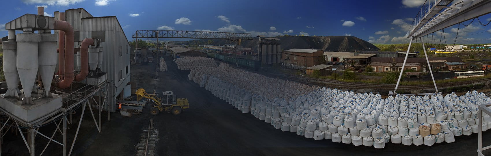
Understanding the cost and pricing dynamics for sourcing silicon conductive materials is essential for international B2B buyers aiming to optimize procurement strategies. The pricing structure is influenced by multiple factors spanning from raw materials to delivery terms, each impacting the final cost and value proposition.
Raw Materials: The primary input is silicon, often combined with conductive additives such as carbon or metal particles. The purity and grade of silicon substantially affect cost, with higher-grade silicon commanding premium pricing due to improved conductivity and reliability.
Labor Costs: Manufacturing labor varies significantly by region. Facilities in Europe or the Middle East may have higher labor costs compared to those in Africa or South America. Skilled labor for precision manufacturing and quality assurance is a critical cost driver.
Manufacturing Overhead: Includes energy consumption, equipment depreciation, factory maintenance, and administrative expenses. Silicon processing can be energy-intensive, especially in refining and doping stages, influencing overhead costs.
Tooling and Equipment: Initial investment in specialized machinery for silicon wafer production or conductive film deposition impacts unit costs, especially for smaller order volumes.
Quality Control (QC): Rigorous testing for conductivity, durability, and compliance with international standards adds to costs but is vital for ensuring product performance and customer satisfaction.
Logistics and Shipping: Transporting silicon conductive materials internationally involves customs duties, freight charges, insurance, and handling fees. The choice of Incoterms greatly affects cost allocation and risk.
Profit Margin: Suppliers incorporate margins based on market demand, competition, and order size, influencing final pricing.
Order Volume and Minimum Order Quantity (MOQ): Larger volumes typically attract volume discounts, reducing per-unit cost. Buyers from emerging markets like Kenya or Vietnam can leverage consolidated orders to negotiate better pricing.
Specifications and Customization: Customized silicon conductive materials with specific conductivity levels, thickness, or form factors increase costs due to specialized processing and lower economies of scale.
Material Quality and Certifications: Compliance with certifications such as RoHS, REACH, or ISO standards can raise costs but are often non-negotiable for quality-conscious buyers, especially in Europe and the Middle East.
Supplier Capabilities and Reputation: Established suppliers with robust R&D, consistent quality, and reliable delivery often price higher but reduce risks of defects and delays.
Incoterms Selection: Terms such as FOB, CIF, or DDP influence who bears shipping and customs costs, affecting the landed price. Buyers should carefully select terms aligned with their logistics capabilities.
Negotiate on Volume and Terms: Buyers should aggregate demand to meet or exceed MOQs and negotiate flexible payment and delivery terms to improve pricing.
Evaluate Total Cost of Ownership (TCO): Beyond unit price, consider installation, maintenance, defect rates, and lifecycle costs. Higher upfront costs may translate into long-term savings with superior materials.
Leverage Local and Regional Suppliers: For buyers in Africa, South America, or the Middle East, sourcing from regional suppliers can reduce logistics costs and lead times.
Request Samples and Certifications: Verify material performance and compliance before committing to large orders to avoid costly returns or non-compliance penalties.
Understand Pricing Nuances: Currency fluctuations, tariffs, and geopolitical factors can impact pricing unpredictably. Maintain open communication with suppliers and consider hedging strategies.
Use Clear Incoterms: Define responsibilities clearly to avoid unexpected costs at customs or during transit.
Disclaimer: Pricing for silicon conductive materials varies widely depending on supplier, specifications, and market conditions. The insights provided are indicative and should be supplemented with direct supplier quotations and market research tailored to specific sourcing needs.
For international B2B buyers evaluating silicon's conductive properties, understanding specific technical specifications is essential to ensure material suitability and optimize supply chain efficiency.
Material Grade
Silicon used in conductive applications varies from industrial-grade to semiconductor-grade. Semiconductor-grade silicon has higher purity (99.9999% or more), critical for electronics manufacturing, while industrial-grade may suffice for less sensitive applications. Buyers should specify the grade to match their technical and quality requirements.
Resistivity (Ω·cm)
Resistivity indicates how strongly silicon opposes electric current. Lower resistivity means higher conductivity. Typical resistivity values for conductive silicon range from 0.001 to 10 Ω·cm, depending on doping levels. Understanding resistivity helps buyers assess performance in devices like sensors or photovoltaic cells.
Doping Type and Concentration
Silicon’s conductivity is controlled by doping—adding impurities such as phosphorus (n-type) or boron (p-type). The doping concentration directly affects electrical properties. Buyers must clarify doping specifications to ensure compatibility with their electronic components or manufacturing processes.
Thermal Conductivity (W/m·K)
Thermal conductivity is important for heat dissipation in electronic devices. Silicon’s thermal conductivity varies with purity and doping but generally ranges from 100 to 150 W/m·K. For applications in high-power electronics, selecting silicon with optimal thermal properties prevents overheating and improves reliability.
Physical Dimensions and Tolerances
Silicon wafers or components come in standard thicknesses and diameters, with tight tolerances (±0.01 mm or better). Precise dimensions are crucial for integration into assembly lines and maintaining product consistency. Buyers should verify size specifications and tolerance limits with suppliers to avoid production issues.
Surface Finish and Passivation
The surface condition affects conductivity and device performance. Passivation layers may be applied to protect silicon surfaces from oxidation or contamination. Specifying surface finish requirements ensures material longevity and functionality in end-use environments.
Navigating international trade for silicon conductive materials involves familiarity with key terms that streamline communication and transaction clarity.
OEM (Original Equipment Manufacturer)
Refers to companies that produce parts or components used in another company’s final product. In silicon procurement, buyers may source materials directly from OEMs to ensure quality and traceability.
MOQ (Minimum Order Quantity)
The smallest quantity a supplier is willing to sell. MOQs vary widely and impact inventory planning and cost efficiency. Buyers from emerging markets should negotiate MOQs to balance supply availability with capital constraints.
RFQ (Request for Quotation)
A formal inquiry sent to suppliers to obtain pricing and terms for specific silicon materials. A detailed RFQ including technical specs and delivery timelines helps buyers receive competitive and accurate offers.
Incoterms (International Commercial Terms)
Standardized trade terms defining responsibilities between buyers and sellers for shipping, risk, and costs. Common terms include FOB (Free on Board), CIF (Cost, Insurance, Freight), and DDP (Delivered Duty Paid). Understanding Incoterms is vital for managing logistics and budgeting in cross-border transactions.
Lead Time
The period from order placement to delivery. Silicon production can have long lead times due to manufacturing complexity. Buyers should account for lead times in project schedules and negotiate with suppliers to avoid delays.
Certification and Compliance
Certifications such as ISO 9001 or RoHS compliance indicate quality management and environmental standards adherence. Ensuring suppliers provide certified materials reduces risks related to quality defects or regulatory non-compliance.
For B2B buyers in Africa, South America, the Middle East, and Europe, mastering these technical properties and trade terms is key to selecting the right silicon conductive materials and establishing reliable supplier relationships. Clear communication of specifications and contractual terms minimizes operational risks and supports successful international procurement.
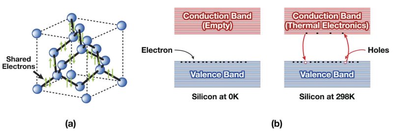
The question of whether silicon is conductive is pivotal in sectors ranging from electronics manufacturing to renewable energy technologies. Silicon, in its pure crystalline form, is a semiconductor—meaning it has conductivity between that of a conductor and an insulator. This unique property allows it to be the foundational material for integrated circuits, solar cells, and various sensors.
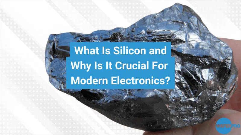
Illustrative Image (Source: Google Search)
Globally, demand for silicon-based components is surging, driven by rapid digitalization, the expansion of Internet of Things (IoT) devices, and the growth of clean energy infrastructure. For B2B buyers in Africa, South America, the Middle East, and Europe, this translates into opportunities and challenges shaped by regional market dynamics:
Key sourcing trends include a growing preference for suppliers who can provide high-purity silicon wafers with consistent quality, alongside advanced doping and surface treatment capabilities. Additionally, vertical integration—where suppliers control multiple stages of silicon refinement and chip manufacturing—is gaining traction to reduce dependency on fluctuating global supply chains.
International buyers must also monitor geopolitical influences, such as trade policies impacting silicon exports, and invest in supplier diversification to mitigate risks. Collaborations with regional partners, especially in Africa and Southeast Asia (e.g., Vietnam), are becoming strategic to access emerging markets and optimize logistics.
Sustainability has become a critical factor in the silicon supply chain, driven by both regulatory pressures and corporate responsibility mandates. Silicon production involves energy-intensive processes, including quartz mining, purification, and crystal growth, which can contribute significantly to carbon emissions and environmental degradation if unmanaged.
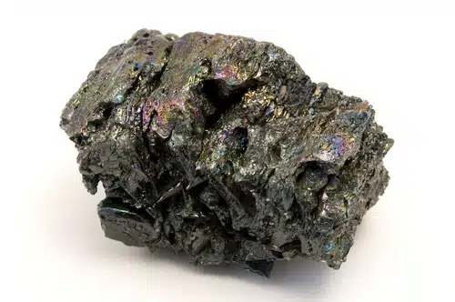
Illustrative Image (Source: Google Search)
For international B2B buyers, prioritizing ethical sourcing means engaging with suppliers who demonstrate:
Moreover, the push for “green silicon”—produced through low-carbon methods and recyclable materials—is gaining momentum. Buyers increasingly demand silicon materials with a reduced environmental footprint to meet their own sustainability goals and those of their clients.
In regions such as Europe, sustainability regulations compel suppliers to reduce waste and emissions, while buyers in Africa and the Middle East are encouraged to develop local industries aligned with sustainable practices to attract international partnerships. Embracing sustainability not only mitigates risks but also enhances brand reputation and compliance with global ESG (Environmental, Social, and Governance) standards.
The conductive properties of silicon were first scientifically characterized in the early 20th century, laying the groundwork for the semiconductor revolution. Initially considered a poor conductor, it was the discovery of doping techniques—adding impurities to silicon crystals—that enabled controlled conductivity essential for electronic devices.
This breakthrough transformed silicon into the backbone of modern electronics, from transistors to microprocessors. Over decades, silicon’s role expanded into photovoltaics, powering the global solar industry. Understanding silicon’s conductivity evolution provides B2B buyers insight into supplier capabilities, especially regarding advanced material engineering and custom semiconductor solutions tailored to specific industrial needs.
Is silicon conductive and how does this property affect its industrial applications?
Silicon is a semiconductor, meaning it has electrical conductivity between that of a conductor and an insulator. This unique property allows it to control electrical current flow, making it essential for electronics, photovoltaics, and sensor industries. For B2B buyers, understanding silicon’s conductivity helps in selecting the right grade and form—such as monocrystalline or polycrystalline silicon—to match specific applications like solar panels or microchips, optimizing performance and cost-efficiency.
How should international B2B buyers vet silicon suppliers to ensure product quality and reliability?
Due diligence is critical. Buyers should verify suppliers’ certifications (e.g., ISO 9001, RoHS compliance), request detailed technical datasheets, and assess their production capacity and quality control processes. Conducting factory audits or third-party inspections can uncover manufacturing standards and traceability. Engaging with suppliers who have proven export experience to regions like Africa or Europe ensures smoother customs clearance and regulatory compliance, reducing risks in international trade.
Can silicon materials be customized for specific conductivity or purity requirements?
Yes, silicon can be tailored in terms of purity levels, doping elements, and physical form to meet precise electrical and mechanical specifications. Buyers should communicate their technical requirements clearly, including resistivity, crystal structure, and wafer dimensions. Working with suppliers offering R&D collaboration or flexible production batches helps achieve optimal customization, particularly important for industries requiring high-performance silicon such as semiconductors or advanced electronics.
What are typical minimum order quantities (MOQs), lead times, and payment terms for silicon conductive materials in international trade?
MOQs vary widely depending on the silicon type and supplier, ranging from small prototype quantities to large industrial volumes. Lead times can span from a few weeks to several months, especially for high-purity or specialized silicon products. Payment terms commonly include letters of credit or advance payments to secure orders, particularly for new international buyers. Negotiating favorable terms requires transparent communication and often leveraging long-term contracts for better pricing and delivery commitments.
Which quality assurance (QA) certifications and tests should B2B buyers require for conductive silicon?
Key certifications include ISO 9001 for quality management, ISO/TS 16949 for automotive-grade silicon, and compliance with environmental standards like RoHS and REACH. Buyers should also insist on batch-specific testing reports covering electrical resistivity, impurity levels, and crystallographic analysis. Independent lab testing or supplier-provided certificates of analysis (COA) reduce the risk of receiving substandard materials, ensuring product consistency and compliance with industry regulations.
What logistics considerations are essential when importing silicon conductive materials to Africa, South America, the Middle East, or Europe?
Silicon products often require careful packaging to prevent contamination and damage, especially wafers or thin films. Buyers should choose freight options balancing cost and transit time, considering customs clearance procedures in target regions. Utilizing experienced freight forwarders and understanding local import regulations, tariffs, and documentation (e.g., commercial invoice, certificate of origin) will minimize delays. For perishable or sensitive silicon forms, temperature-controlled shipping may be necessary.
How can B2B buyers mitigate risks related to disputes or product non-conformance in international silicon procurement?
Including clear contract terms covering quality specifications, inspection rights, and dispute resolution mechanisms (e.g., arbitration clauses) is vital. Buyers should insist on third-party pre-shipment inspections and maintain open communication channels with suppliers. Establishing strong relationships and using escrow payment services can protect financial interests. Promptly documenting and reporting any non-conformance facilitates faster remediation, including replacement shipments or refunds.
Are there regional market trends affecting the supply and demand of conductive silicon for B2B buyers?
Yes, demand is growing globally due to expanding renewable energy and electronics sectors, with significant market activity in Europe, the Middle East, and emerging African and South American markets. Buyers should monitor geopolitical factors, trade tariffs, and raw material availability that impact silicon pricing and supply chains. Sourcing from diversified suppliers and staying informed about innovations like silicon carbide or alternative semiconductors can provide competitive advantages in rapidly evolving markets.
The information provided in this guide, including content regarding manufacturers, technical specifications, and market analysis, is for informational and educational purposes only. It does not constitute professional procurement advice, financial advice, or legal advice.
While we have made every effort to ensure the accuracy and timeliness of the information, we are not responsible for any errors, omissions, or outdated information. Market conditions, company details, and technical standards are subject to change.
B2B buyers must conduct their own independent and thorough due diligence before making any purchasing decisions. This includes contacting suppliers directly, verifying certifications, requesting samples, and seeking professional consultation. The risk of relying on any information in this guide is borne solely by the reader.
Silicon’s unique conductive properties position it as a cornerstone material in modern electronics and advanced manufacturing sectors. For international B2B buyers—especially those operating in dynamic markets across Africa, South America, the Middle East, and Europe—understanding silicon’s conductivity nuances is essential for optimizing product performance and supply chain efficiency.
Illustrative Image (Source: Google Search)
Key Takeaways for Strategic Sourcing:
Looking ahead, the demand for silicon with specialized conductive attributes will only grow as industries push toward miniaturization and energy efficiency. Buyers in emerging and established markets alike should adopt a proactive sourcing strategy that combines technical insight with global market intelligence. By doing so, they can secure competitive advantages, foster innovation, and build resilient supply chains that support sustainable growth.
Actionable Next Step: Engage with industry experts and silicon producers early to customize sourcing strategies that align with your operational goals and regional market dynamics. This approach will empower your business to capitalize on silicon’s conductive potential in a rapidly evolving global landscape.
Tags: Black Silicon Carbide, White Fused Alumina, Brown Fused Alumina, Pink Fused Alumina, Black Fused Alumina