Silicon carbide substrate is rapidly becoming a cornerstone material in high-performance electronics, power devices, and advanced semiconductor applications. For international B2B buyers across Africa, South America, the Middle East, and Europe, understanding the complexities of this niche market is essential to securing reliable supply chains and optimizing product performance. As demand grows, so does the need for clear insights into sourcing strategies, product specifications, and supplier capabilities.
This comprehensive guide is designed to equip buyers with actionable knowledge on every critical aspect of silicon carbide substrates. From exploring the different types and material grades to understanding manufacturing processes and quality control standards, it offers a 360-degree view of the market landscape. Additionally, the guide delves into key supplier profiles, cost considerations, and emerging global market trends that impact availability and pricing.
By addressing frequently asked questions and highlighting region-specific sourcing challenges, this resource empowers decision-makers in diverse markets—including Saudi Arabia’s expanding industrial sector and Italy’s advanced manufacturing hubs—to make informed, strategic procurement choices. Whether you are looking to enhance product quality, reduce lead times, or negotiate better terms, the insights provided here will help you navigate the silicon carbide substrate market with confidence and precision.
In a rapidly evolving global supply chain, being well-informed is your strongest asset. This guide serves as a strategic tool to unlock value and foster long-term partnerships in the silicon carbide substrate ecosystem.
| Type Name | Key Distinguishing Features | Primary B2B Applications | Brief Pros & Cons for Buyers |
|---|---|---|---|
| 4H-Silicon Carbide | Hexagonal crystal structure with high electron mobility | Power electronics, high-frequency devices | Pros: Excellent electronic properties, high thermal conductivity; Cons: Higher cost, complex manufacturing |
| 6H-Silicon Carbide | Different hexagonal polytype with lower electron mobility | LEDs, optoelectronics, and some power devices | Pros: Cost-effective for certain optoelectronic uses; Cons: Lower performance in high-power electronics |
| Semi-Insulating SiC | High resistivity due to intentional doping | RF devices, microwave circuits, high-frequency components | Pros: Reduces parasitic conduction, ideal for high-frequency; Cons: Limited availability, specialized applications |
| Epitaxial SiC Substrate | Thin, high-quality SiC layer grown on bulk substrate | Semiconductor wafers for device fabrication | Pros: Superior surface quality, enhances device performance; Cons: Higher production cost, requires precise handling |
| 3C-Silicon Carbide | Cubic crystal structure, lower thermal conductivity | MEMS devices, some niche optoelectronics | Pros: Compatible with silicon, lower cost; Cons: Lower thermal and electronic performance compared to hexagonal types |
4H-Silicon Carbide
4H-SiC is favored for its superior electron mobility and thermal conductivity, making it ideal for demanding power electronics and RF applications. Buyers from regions with growing renewable energy and electric vehicle sectors, such as Europe and the Middle East, will find this substrate highly suitable. Purchasing considerations include higher price points and the need for suppliers capable of consistent high-quality crystal growth.
6H-Silicon Carbide
This polytype offers a balance between cost and performance, commonly used in LEDs and optoelectronics. It suits buyers targeting cost-sensitive applications where ultra-high performance is not critical. For B2B procurement, focus on evaluating supplier reliability and batch consistency, especially in emerging markets like South America and Africa where cost efficiency is prioritized.
Semi-Insulating SiC
Designed with intentional doping to achieve high resistivity, semi-insulating SiC substrates are essential for high-frequency and microwave device manufacturing. Buyers in telecommunications and aerospace sectors, notably in technologically advanced regions such as Europe and the Middle East, should prioritize substrate purity and supplier expertise due to the specialized nature of this material.
Epitaxial SiC Substrate
Epitaxial layers grown on SiC substrates provide a superior surface for semiconductor device fabrication, enhancing device performance significantly. This type is critical for semiconductor fabs investing in high-performance wafer production. International buyers must consider the epitaxial layer thickness, uniformity, and supplier technological capabilities to ensure alignment with device specifications.
3C-Silicon Carbide
With a cubic crystal structure, 3C-SiC offers compatibility with silicon-based processes, making it attractive for MEMS and niche optoelectronic applications. Buyers aiming for integration with existing silicon infrastructure, particularly in emerging tech hubs in Africa and South America, will benefit from its lower cost. However, they should weigh the trade-offs in thermal and electronic performance compared to hexagonal SiC types.
Related Video: How Is Carbide Made?
| Industry/Sector | Specific Application of silicon carbide substrate | Value/Benefit for the Business | Key Sourcing Considerations for this Application |
|---|---|---|---|
| Power Electronics | High-efficiency power devices for electric vehicles (EVs) | Enables higher switching frequencies, reduces energy loss, and improves thermal management | Ensure substrate uniformity, low defect density, and compatibility with EV-grade semiconductor fabrication |
| Renewable Energy | Photovoltaic (solar) power modules and inverters | Enhances durability and efficiency under high-temperature and high-voltage conditions | Source substrates with high thermal conductivity and mechanical strength suitable for harsh climates |
| Telecommunications | High-frequency RF devices for 5G and satellite communication | Supports higher frequency operation with lower signal loss, enabling faster data transmission | Prioritize substrates with excellent microwave properties and minimal dielectric losses |
| Industrial Automation | High-power industrial motor drives and power converters | Improves energy efficiency and reliability in harsh industrial environments | Focus on substrates with robust thermal stability and resistance to chemical contamination |
| Aerospace & Defense | High-reliability semiconductors for radar and avionics systems | Provides superior performance under extreme temperature and radiation exposure | Verify substrate quality certifications and compliance with aerospace standards |
In the electric vehicle (EV) sector, silicon carbide (SiC) substrates are critical for manufacturing power devices like MOSFETs and diodes. These devices benefit from SiC’s ability to operate at higher voltages and temperatures with lower energy losses compared to silicon. For B2B buyers in regions such as Europe and the Middle East, sourcing SiC substrates with consistent crystalline quality and minimal defects is essential to meet the stringent reliability standards of automotive OEMs. Additionally, suppliers must provide substrates compatible with EV-grade semiconductor processes to ensure seamless integration.
SiC substrates are increasingly used in solar power inverters and photovoltaic modules due to their exceptional thermal conductivity and ability to withstand high voltage stress. This translates to improved system efficiency and longer service life, especially important in regions like Africa and South America where solar installations face harsh environmental conditions. Buyers should prioritize substrates that maintain mechanical strength and performance under prolonged exposure to heat and UV radiation, ensuring stable operation and reducing maintenance costs.
For telecommunications equipment supporting 5G networks and satellite communications, SiC substrates enable high-frequency RF components with reduced signal attenuation. This is vital for achieving the high data throughput and low latency demanded by modern communication infrastructures. International buyers, particularly from technologically advanced markets like Italy and Saudi Arabia, need to select substrates with superior microwave dielectric properties and minimal impurities to optimize device performance and reliability in diverse climatic conditions.
In industrial automation, SiC substrates are used in power converters and motor drives that operate continuously under high power and temperature loads. The robustness of SiC substrates enhances energy efficiency and device longevity, reducing downtime in manufacturing plants. B2B buyers should assess substrate thermal stability and chemical resistance to ensure compatibility with harsh industrial environments, including exposure to dust, oils, and vibration, which are common in factories across South America and the Middle East.
Silicon carbide substrates are indispensable in aerospace and defense applications for radar, avionics, and satellite systems due to their ability to withstand extreme temperatures and radiation. Their use improves device reliability and performance in mission-critical environments. Buyers must ensure that substrates meet rigorous aerospace quality standards and certifications, including traceability and batch consistency, which are critical for procurement in highly regulated markets such as Europe and the Middle East.
Related Video: What is Silicon Carbide?
Key Properties:
Monocrystalline 4H-SiC substrates exhibit excellent thermal conductivity (~490 W/m·K), high breakdown electric field (~2.2 MV/cm), and outstanding chemical inertness. They maintain structural integrity at temperatures exceeding 1600°C and offer superior electron mobility, crucial for high-frequency and high-power electronic devices.
Pros & Cons:
- Pros: Exceptional electronic properties, low defect density, and high thermal stability make it ideal for power electronics and RF applications.
- Cons: High manufacturing complexity and cost due to the precise crystal growth process. Limited wafer sizes can restrict scalability.
Impact on Application:
Ideal for high-performance semiconductor devices, including power transistors and Schottky diodes, where efficiency and heat dissipation are critical. Its chemical resistance suits harsh industrial environments, including chemical processing and aerospace.
International Buyer Considerations:
Buyers in Europe (e.g., Italy) and the Middle East (e.g., Saudi Arabia) should ensure compliance with international semiconductor standards such as ASTM F1856 and JEDEC JESD22 for device reliability. Given the high cost, buyers from emerging markets in Africa and South America must balance performance needs with budget constraints, possibly prioritizing smaller wafer sizes or alternative materials.
Key Properties:
Polycrystalline SiC offers good thermal conductivity (~120-200 W/m·K) and high hardness, with moderate electrical properties compared to monocrystalline forms. It withstands temperatures up to 1400°C and exhibits excellent corrosion resistance.
Pros & Cons:
- Pros: Lower cost and easier to manufacture than monocrystalline substrates. Suitable for abrasive and wear-resistant applications.
- Cons: Higher defect density and lower electron mobility limit its use in high-frequency electronics.
Impact on Application:
Commonly used in mechanical seals, wear parts, and substrates for less demanding electronic components. Its robustness makes it suitable for chemical plants and oil & gas industries prevalent in the Middle East and parts of Africa.
International Buyer Considerations:
Buyers should verify compliance with DIN EN ISO 9001 quality management standards and ASTM C799 for mechanical properties. In South America and Africa, where cost-efficiency is critical, polycrystalline SiC offers a practical balance between performance and affordability.
Key Properties:
SSiC substrates are produced by sintering SiC powders, resulting in a dense, hard material with good thermal shock resistance and excellent chemical inertness. Thermal conductivity ranges around 90-120 W/m·K, with high resistance to oxidation and acids.
Pros & Cons:
- Pros: Cost-effective for large-scale production, excellent corrosion resistance, and suitable for harsh chemical environments.
- Cons: Lower mechanical strength and thermal conductivity compared to monocrystalline SiC, limiting use in high-power electronics.
Impact on Application:
Widely used in mechanical seals, pump components, and chemical processing equipment. Its resistance to aggressive media is beneficial for buyers in the Middle East’s petrochemical sectors and European chemical industries.
International Buyer Considerations:
Compliance with ASTM C799 and JIS R 1601 standards is essential. Buyers in Africa and South America can leverage SSiC for industrial applications requiring durability without the premium cost of monocrystalline SiC.
Key Properties:
Epi-SiC involves a thin monocrystalline SiC layer grown on a substrate, combining excellent electronic properties with structural support. It offers high electron mobility and thermal conductivity similar to bulk monocrystalline SiC.
Pros & Cons:
- Pros: Enables high-quality semiconductor device fabrication with reduced defect densities. Enhances device performance in power and RF applications.
- Cons: Complex and costly production process, requiring advanced equipment and expertise.
Impact on Application:
Critical for advanced semiconductor devices, including high-voltage power modules and high-frequency transistors. Its use is prevalent in automotive electronics and renewable energy sectors, which are growing markets in Europe and the Middle East.
International Buyer Considerations:
Buyers must ensure suppliers adhere to strict JEDEC and IEC semiconductor standards. The high cost and technical requirements may limit accessibility for buyers in developing regions unless supported by government or industry partnerships.
| Material | Typical Use Case for silicon carbide substrate | Key Advantage | Key Disadvantage/Limitation | Relative Cost (Low/Med/High) |
|---|---|---|---|---|
| Monocrystalline Silicon Carbide (4H-SiC) | High-power electronics, RF devices, harsh environments | Superior thermal/electrical properties | High manufacturing cost and limited wafer size | High |
| Polycrystalline Silicon Carbide (β-SiC) | Mechanical seals, wear parts, moderate electronics | Cost-effective, robust, good corrosion resistance | Lower electron mobility and higher defects | Medium |
| Sintered Silicon Carbide (SSiC) | Chemical processing equipment, industrial seals | Excellent chemical resistance, cost-effective | Lower mechanical strength and thermal conductivity | Low |
| Epitaxial Silicon Carbide (Epi-SiC) | Advanced semiconductor devices, power modules | High-quality electronic layer, enhanced device performance | Complex and costly production process | High |
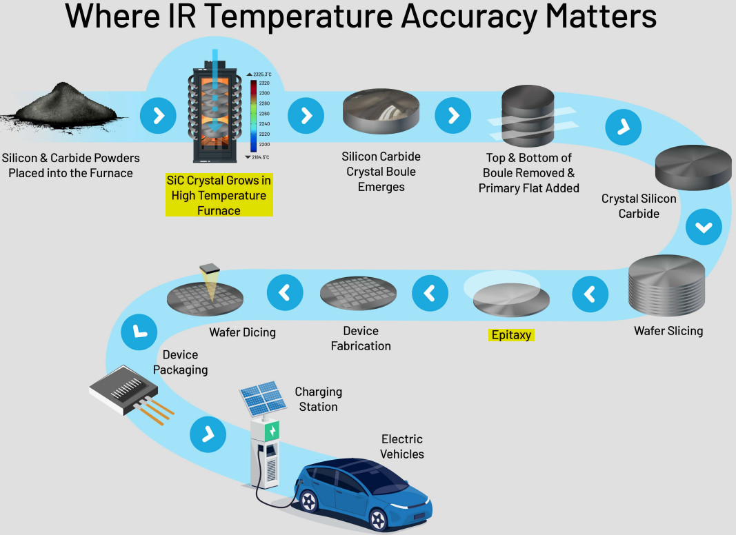
Silicon carbide (SiC) substrates are critical components in high-performance power electronics, demanding precise and controlled manufacturing processes to ensure superior material properties. Understanding these processes enables B2B buyers to assess supplier capabilities and product quality effectively.

Illustrative Image (Source: Google Search)
1. Material Preparation
The process begins with the synthesis of high-purity silicon carbide material, usually through the chemical vapor deposition (CVD) or physical vapor transport (PVT) methods. Raw materials must meet stringent purity levels (often 99.999% or higher) to minimize defects. In this stage, silicon and carbon sources are carefully selected and purified to avoid contamination that can affect electrical and mechanical properties.
2. Crystal Growth and Forming
The core forming stage involves growing large, single-crystal SiC boules using the PVT technique, where SiC powder sublimates at high temperatures (~2500°C) in a controlled environment and recrystallizes on a seed crystal. This step demands precise thermal management and atmosphere control to reduce crystal defects such as micropipes and dislocations. Boules are typically grown in various polytypes, with 4H-SiC being the most common for power applications.
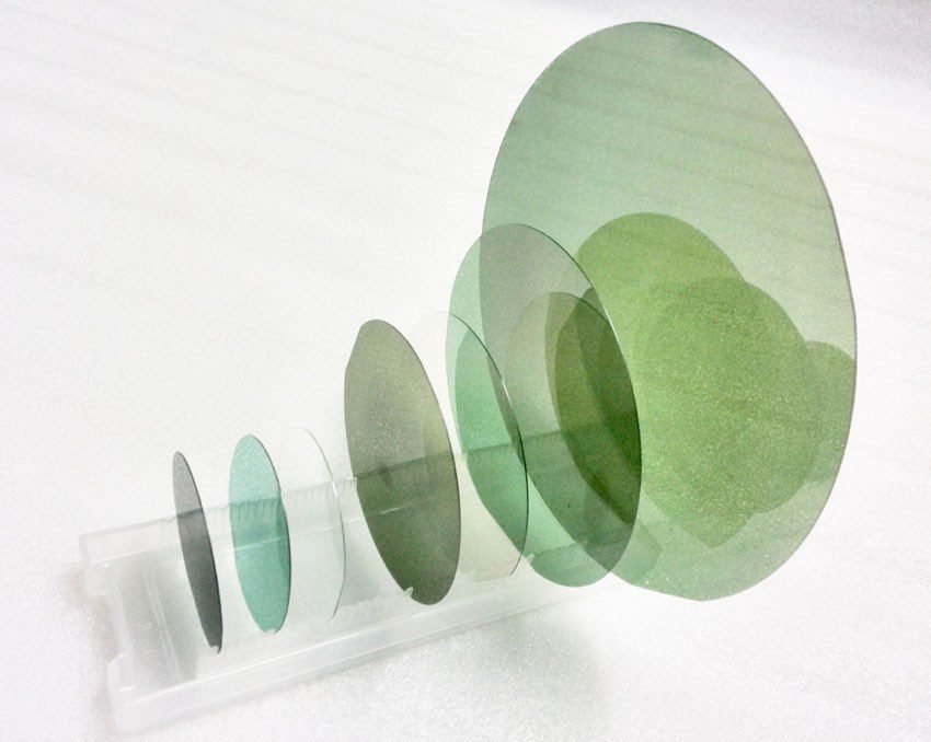
3. Wafer Slicing and Lapping
After boule growth, the material is sliced into thin wafers using diamond wire saws or laser cutting. This step requires high precision to maintain thickness uniformity and avoid micro-cracks. Subsequent lapping and polishing processes refine wafer surfaces, achieving the smoothness and flatness essential for device fabrication.
4. Surface Treatment and Finishing
Final finishing involves chemical mechanical polishing (CMP) to remove surface damage and achieve atomic-level smoothness. Some manufacturers also perform epitaxial layer deposition on the substrate to provide tailored electrical characteristics for specific applications. The finished wafers undergo cleaning and packaging in clean-room environments to prevent contamination.
Quality assurance (QA) in SiC substrate manufacturing is multi-tiered and aligned with international standards to ensure product reliability, especially for demanding industrial and automotive sectors.
Relevant Standards and Certifications
- ISO 9001: The foundational quality management standard, ensuring consistent manufacturing processes and continuous improvement.
- IATF 16949: Crucial for automotive-related SiC substrates, addressing stringent quality requirements.
- CE Marking: Required for products sold in Europe, indicating compliance with health, safety, and environmental protection standards.
- Industry-specific standards: Depending on application, such as API (American Petroleum Institute) standards for energy sectors, or RoHS compliance for environmental regulations.
1. Incoming Quality Control (IQC)
Suppliers inspect raw materials and components for purity, particle size, and contamination levels. Spectroscopic analysis (e.g., ICP-MS, SIMS) is common to verify chemical composition.
2. In-Process Quality Control (IPQC)
This includes monitoring crystal growth parameters, boule integrity via X-ray topography, and wafer thickness measurements. Real-time process control systems help detect deviations early.
3. Final Quality Control (FQC)
Finished wafers undergo comprehensive testing:
- Surface morphology via atomic force microscopy (AFM) or scanning electron microscopy (SEM).
- Electrical testing for carrier lifetime and resistivity.
- Defect density analysis using photoluminescence or etching techniques.
- Flatness and thickness uniformity measurements using interferometry.
- Mechanical strength tests to assess wafer robustness.
For buyers in Africa, South America, the Middle East, and Europe, verifying supplier quality systems is critical due to geographical and regulatory differences.
1. Conducting On-Site Audits
Request and schedule factory audits focusing on process controls, equipment calibration, employee training, and cleanliness protocols. Audits should verify compliance with ISO 9001 or equivalent certifications and assess traceability mechanisms.
2. Reviewing Quality Documentation and Reports
Demand detailed quality control reports, including batch traceability, test results, and non-conformance records. Consistent documentation reflects mature quality management and transparency.
3. Utilizing Third-Party Inspection Services
Engage independent inspection agencies specializing in semiconductor materials to conduct random sample testing and certification. This adds an unbiased verification layer, especially valuable when dealing with new or distant suppliers.
By thoroughly evaluating manufacturing processes and quality assurance practices, international B2B buyers can secure silicon carbide substrates that meet their performance, reliability, and regulatory needs, ensuring successful integration into advanced electronic applications.
When sourcing silicon carbide (SiC) substrates, international B2B buyers must dissect the underlying cost components to make informed procurement decisions. The primary cost drivers include:
Pricing for SiC substrates is not static and depends on several critical factors:
For buyers in Africa, South America, the Middle East, and Europe, optimizing cost-efficiency requires strategic negotiation and holistic evaluation:
Pricing for silicon carbide substrates can vary widely based on technical specifications, order size, and market conditions. The figures discussed herein are indicative and should not be considered final quotations. Buyers are advised to request tailored proposals and conduct comparative analysis across multiple suppliers to secure optimal value.
By understanding the nuanced cost structure and pricing drivers, international B2B buyers can strategically navigate the silicon carbide substrate market, ensuring competitive procurement aligned with technical and financial objectives.
When sourcing silicon carbide (SiC) substrates, understanding the core technical specifications is essential for ensuring compatibility with your manufacturing processes and end-product requirements. Below are critical properties that international buyers, especially from emerging and developed markets, should prioritize:
Material Grade
Silicon carbide substrates come in various polytypes, primarily 4H-SiC and 6H-SiC. The 4H polytype is preferred for high-performance power electronics due to superior electron mobility. Selecting the correct grade impacts device efficiency and thermal performance, directly influencing product competitiveness.
Wafer Diameter and Thickness Tolerance
Standard diameters range from 100 mm to 150 mm, with tight thickness tolerances (often ±25 µm or better). Consistent wafer size and thickness ensure uniformity in device fabrication and reduce waste. For B2B buyers, confirming these tolerances upfront minimizes integration issues with downstream processes.
Crystalline Quality (Dislocation Density)
The density of crystal defects such as micropipes and dislocations affects yield and reliability. Lower dislocation densities translate into higher device performance and longer lifetimes. Buyers should request detailed defect density metrics to assess substrate quality.
Surface Finish and Polishing
Substrates typically have a polished surface finish to nanometer-scale roughness, crucial for epitaxial layer growth. The surface condition impacts device layer uniformity and electrical characteristics. Clarify surface finish standards to align with your fabrication requirements.
Doping and Resistivity
Intrinsic or lightly doped substrates with specific resistivity ranges (e.g., >10^5 Ω·cm for semi-insulating types) are used depending on the device application. Understanding doping levels helps in selecting substrates compatible with power devices or RF components.
Thermal Conductivity
SiC substrates have high thermal conductivity (~490 W/m·K), superior to silicon, aiding heat dissipation in high-power devices. This property is critical for applications in harsh environments or where thermal management is a priority.
Navigating the silicon carbide substrate market requires familiarity with key trade and industry terminology. Here are terms every international buyer should know to streamline communication and contract negotiations:
OEM (Original Equipment Manufacturer)
Refers to companies that incorporate silicon carbide substrates into their final products. Understanding if your supplier works directly with OEMs can indicate product quality and supply chain reliability.
MOQ (Minimum Order Quantity)
The smallest quantity a supplier is willing to sell. MOQs can vary significantly, especially for specialized substrates. Buyers from emerging markets should negotiate MOQs that align with their production scale to optimize inventory costs.
RFQ (Request for Quotation)
A formal inquiry sent to suppliers to obtain pricing and terms. Preparing detailed RFQs with specifications like wafer size, grade, and tolerances ensures accurate quotes and helps compare multiple vendors efficiently.
Incoterms (International Commercial Terms)
Standardized trade terms defining responsibilities for shipping, insurance, and customs between buyer and seller. Common terms include FOB (Free on Board) and CIF (Cost, Insurance, and Freight). Knowing Incoterms helps buyers manage logistics risks and costs effectively.
Epi-ready
Indicates that the substrate surface is polished and prepared for epitaxial layer deposition without further treatment. Specifying “epi-ready” substrates avoids additional processing steps, saving time and cost.
Yield
The percentage of usable substrates or devices produced from a batch. High yield rates are critical for cost-efficiency. Buyers should inquire about typical yield statistics and quality control processes.
By mastering these technical properties and trade terms, international B2B buyers can make informed decisions, optimize procurement strategies, and ensure their silicon carbide substrate supply meets both performance and commercial expectations. This knowledge is especially valuable for markets in Africa, South America, the Middle East, and Europe, where balancing quality with cost and supply chain reliability is paramount.
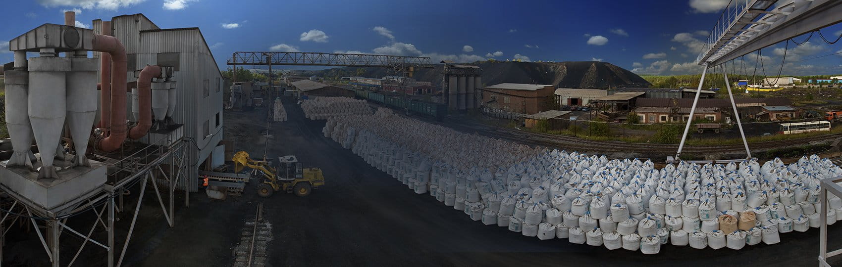
The silicon carbide (SiC) substrate market is experiencing robust growth driven by the expanding demand for high-efficiency power electronics, particularly in automotive, renewable energy, and industrial sectors. For international B2B buyers from regions such as Africa, South America, the Middle East, and Europe, understanding the global market drivers and sourcing trends is crucial for strategic procurement.
Key growth drivers include the accelerating adoption of electric vehicles (EVs) and renewable energy systems, where SiC substrates enable higher switching frequencies, lower energy losses, and improved thermal management. Europe, led by countries like Italy, is heavily investing in green technologies, increasing the demand for SiC substrates in power modules and inverters. Similarly, Middle Eastern markets such as Saudi Arabia are focusing on diversifying their energy portfolios, fostering opportunities for SiC-based solutions in solar and smart grid applications.
From a sourcing perspective, B2B buyers are witnessing a shift towards vertically integrated supply chains, with a focus on securing high-quality, defect-free substrates. The market favors suppliers offering customization capabilities, shorter lead times, and strong technical support. Additionally, partnerships and joint ventures between substrate manufacturers and device producers are becoming prevalent to mitigate supply risks and accelerate innovation.
Emerging trends include the rise of 200 mm wafer sizes, which promise cost efficiencies and scalability, and the integration of advanced crystal growth techniques that enhance substrate uniformity and performance. Buyers should also monitor geopolitical factors influencing supply chains, such as trade policies and regional manufacturing hubs, to optimize sourcing strategies.
Illustrative Image (Source: Google Search)
Sustainability is increasingly pivotal in the silicon carbide substrate sector, reflecting growing environmental regulations and corporate responsibility commitments worldwide. For B2B buyers, especially those operating in environmentally conscious markets like Europe and progressive regions in the Middle East, aligning procurement with sustainability goals is essential.
The production of SiC substrates involves energy-intensive processes such as high-temperature crystal growth and wafer polishing, which contribute to carbon emissions. Leading manufacturers are adopting renewable energy sources, waste reduction protocols, and water recycling methods to mitigate environmental impact. Buyers should prioritize suppliers that disclose environmental performance metrics and hold certifications such as ISO 14001 (Environmental Management) or adhere to recognized green manufacturing standards.
Ethical sourcing extends beyond environmental concerns to include responsible supply chain practices. This encompasses conflict-free raw material sourcing, fair labor conditions, and transparent supplier audits. Given the global nature of SiC substrate supply chains, buyers from Africa, South America, and other regions should ensure their partners comply with internationally accepted ethical standards to avoid reputational risks and foster long-term partnerships.
Illustrative Image (Source: Google Search)
Moreover, the emergence of “green” SiC substrates—manufactured using cleaner processes and recyclable materials—is gaining traction. B2B buyers can leverage these innovations to meet client demands for sustainable components and enhance their own ESG (Environmental, Social, Governance) profiles.
Silicon carbide substrates have evolved significantly since their inception in the 1980s when they were primarily niche materials for high-temperature electronics. Initially challenged by high production costs and limited wafer sizes, advancements in crystal growth technologies such as Physical Vapor Transport (PVT) and improvements in wafer polishing have made SiC substrates commercially viable for mainstream power electronics.
The transition from 100 mm to 150 mm wafers marked a critical milestone, enabling greater production scale and cost reduction. Currently, the industry is advancing towards 200 mm wafers, promising further economies of scale and enhanced device performance. This evolution reflects the substrate’s expanding role in enabling next-generation power devices that support global decarbonization and energy efficiency initiatives.
For B2B buyers, understanding this historical context helps in assessing supplier capabilities and future readiness, particularly when evaluating long-term contracts or investments in emerging technologies.
1. How can I effectively vet silicon carbide substrate suppliers internationally?
Start by verifying the supplier’s industry certifications such as ISO 9001 or IATF 16949, which demonstrate adherence to quality management standards. Request product samples and detailed technical datasheets to assess material quality. Evaluate their manufacturing capacity and past client references, especially from regions similar to yours in terms of regulatory and environmental conditions. For buyers in Africa, South America, the Middle East, and Europe, consider suppliers with established export experience to your region to ensure smoother customs and logistics processes. Conduct virtual or onsite audits where possible to confirm compliance with your specifications.
2. What customization options are typically available for silicon carbide substrates?
Most manufacturers offer customization in terms of wafer diameter, thickness, crystal orientation, doping concentration, and surface finish. Discuss your specific application requirements upfront to ensure the substrate meets electrical, thermal, and mechanical performance needs. For international buyers, clarify if customization affects minimum order quantities (MOQ) or lead times. Suppliers in Europe and the Middle East often provide advanced customization, including epitaxial layer integration. Ensure customization agreements are clearly documented in the contract to avoid misunderstandings during production.
3. What are common MOQ and lead time expectations for international orders?
MOQ can vary widely depending on substrate size, customization, and supplier capacity, often ranging from a few dozen to several hundred wafers per order. Lead times typically span 4 to 12 weeks but may extend based on complexity and shipping logistics. Buyers from regions with longer import clearance times, such as Africa or South America, should factor in additional buffer time. Negotiate flexible MOQ or staggered deliveries if you require smaller quantities initially. Confirm lead times in writing and monitor production milestones to avoid supply chain disruptions.
4. Which payment terms are standard when sourcing silicon carbide substrates internationally?
Common payment terms include Letters of Credit (LC), Telegraphic Transfers (T/T), and open accounts with net payment periods (30-90 days). LCs provide security for both parties but involve bank fees and processing time. T/T upfront payments are typical for first-time orders or smaller buyers. Established buyers, especially in Europe and the Middle East, may negotiate extended payment terms based on trust and volume. Always ensure payment terms are clearly outlined in your purchase agreement, and consider currency fluctuation risks when dealing with suppliers in different regions.
5. What quality assurance and certifications should I require from suppliers?
Request suppliers to provide certificates of analysis (COA) for each batch, detailing critical parameters like purity, resistivity, and defect density. Industry certifications like ISO 9001, ISO 14001, and RoHS compliance are crucial for environmental and quality assurance. For high-reliability applications, look for additional certifications such as IATF 16949 or compliance with JEDEC standards. International buyers should also verify that the supplier’s quality management system supports traceability and continuous improvement. Regular third-party testing or audits can reinforce confidence in product consistency.
6. How can I manage logistics and customs challenges when importing silicon carbide substrates?
Partner with freight forwarders experienced in handling semiconductor materials to ensure proper packaging, temperature control, and documentation. Be aware of import regulations and tariffs specific to your country—African and South American buyers often face variable customs clearance times and duties. Use Incoterms like DAP or DDP to clarify responsibility for shipping costs and risks. Establish clear communication channels with your supplier and logistics partners to track shipments proactively and resolve delays quickly. Investing in customs brokerage services can streamline import clearance.
7. What steps should I take if a dispute arises with an international silicon carbide substrate supplier?
Begin with direct communication to clarify the issue, supported by documented evidence such as quality reports, contracts, and correspondence. Utilize dispute resolution clauses in your contract, which may specify mediation or arbitration venues, often in neutral countries or under ICC rules. For buyers in Europe or the Middle East, international commercial arbitration is common and enforceable. Avoid escalating disputes without professional legal advice familiar with international trade laws. Maintaining a collaborative relationship can often lead to amicable solutions without lengthy litigation.
8. How can I ensure long-term supply stability for silicon carbide substrates in volatile markets?
Diversify your supplier base across regions to mitigate risks from geopolitical disruptions, trade restrictions, or natural disasters. Establish strategic partnerships with suppliers who demonstrate capacity flexibility and innovation capabilities. Negotiate framework agreements with volume commitments and agreed price structures to secure priority production slots. Regularly review your supply chain risks and incorporate buffer stocks if feasible. For buyers in emerging markets like Africa and South America, leveraging local trade agreements or free trade zones can reduce costs and improve supply reliability.
The information provided in this guide, including content regarding manufacturers, technical specifications, and market analysis, is for informational and educational purposes only. It does not constitute professional procurement advice, financial advice, or legal advice.
While we have made every effort to ensure the accuracy and timeliness of the information, we are not responsible for any errors, omissions, or outdated information. Market conditions, company details, and technical standards are subject to change.
B2B buyers must conduct their own independent and thorough due diligence before making any purchasing decisions. This includes contacting suppliers directly, verifying certifications, requesting samples, and seeking professional consultation. The risk of relying on any information in this guide is borne solely by the reader.
Silicon carbide substrates represent a critical foundation for advancing power electronics, automotive, and renewable energy technologies globally. For B2B buyers across Africa, South America, the Middle East, and Europe, strategic sourcing is essential to navigate supply chain complexities, ensure quality, and secure competitive pricing. Prioritizing suppliers with proven technical expertise, scalable production capabilities, and compliance with international standards will mitigate risks and support long-term innovation.
Key takeaways for international buyers include:
Looking ahead, the silicon carbide substrate market is poised for significant growth driven by increasing demand for energy-efficient solutions and electric vehicle adoption. Buyers from regions like Saudi Arabia and Italy are uniquely positioned to capitalize on this momentum by adopting proactive sourcing strategies that emphasize collaboration, innovation, and resilience. Embracing these principles will not only secure supply but also unlock competitive advantages in rapidly evolving industries.
Now is the time to strengthen your sourcing frameworks, deepen supplier relationships, and invest in future-ready materials to drive sustainable growth and technological leadership.
Tags: Black Silicon Carbide, White Fused Alumina, Brown Fused Alumina, Pink Fused Alumina, Black Fused Alumina