The global demand for silicon materials with superior electrical conductivity is rapidly escalating, driven by advancements in electronics, renewable energy, and semiconductor industries. For B2B buyers across Africa, South America, the Middle East, and Europe—including key markets like Italy and Argentina—understanding the nuances of silicon’s conductive properties is essential to secure competitive advantages in product innovation and supply chain efficiency.
Silicon’s ability to conduct electricity underpins critical technologies such as integrated circuits, solar cells, and power electronics. However, sourcing the right type of silicon with optimal conductivity requires deep insight into material grades, doping processes, manufacturing standards, and quality control protocols. Variations in these factors directly impact performance, reliability, and cost-effectiveness—parameters that international buyers must evaluate meticulously.
This comprehensive guide delivers a 360-degree view of the silicon conductivity market, offering actionable intelligence on:
By integrating technical expertise with market dynamics, this guide empowers B2B buyers to make informed sourcing decisions, optimize procurement strategies, and mitigate risks in cross-border transactions. Whether you operate in emerging African tech hubs, South American manufacturing centers, Middle Eastern innovation zones, or established European markets, this resource is designed to enhance your competitive positioning in the evolving silicon conductivity landscape.
| Type Name | Key Distinguishing Features | Primary B2B Applications | Brief Pros & Cons for Buyers |
|---|---|---|---|
| Intrinsic Silicon | Pure silicon with minimal impurities | High-precision semiconductors, research | + High purity, ideal for experimentation - Lower conductivity, higher cost |
| N-type Silicon | Silicon doped with elements like phosphorus (adds electrons) | Microchips, solar cells, electronic devices | + Enhanced conductivity, stable performance - More expensive than intrinsic silicon |
| P-type Silicon | Silicon doped with elements like boron (creates holes) | Transistors, integrated circuits, power devices | + Good electrical conductivity, widely used - Slightly less stable than n-type in some conditions |
| Amorphous Silicon | Non-crystalline silicon, flexible form | Thin-film solar panels, LCD displays | + Cost-effective, flexible substrates - Lower efficiency, less durable |
| Polycrystalline Silicon | Composed of multiple small silicon crystals | Solar panels, large-scale electronics | + Cheaper than monocrystalline, scalable - Lower efficiency than monocrystalline silicon |
Intrinsic Silicon
Intrinsic silicon is the purest form of silicon with very low impurity levels, providing a baseline electrical conductivity. It is primarily used in research and high-precision semiconductor applications where material purity is crucial. For B2B buyers, intrinsic silicon offers excellent control over electrical properties but comes with higher costs and lower conductivity, making it less suitable for mass production or standard electronics manufacturing.
N-type Silicon
N-type silicon is doped with pentavalent impurities such as phosphorus, which introduce free electrons, enhancing conductivity. This type is widely used in microchips, solar cells, and various electronic components requiring reliable and efficient electron flow. Buyers should consider its higher cost relative to intrinsic silicon but benefit from improved electrical performance and stability, making it ideal for advanced electronics manufacturing.
P-type Silicon
P-type silicon is doped with trivalent elements like boron, creating "holes" that act as positive charge carriers. It is a staple in transistor fabrication and integrated circuits, essential for most semiconductor devices. This silicon type balances cost and performance effectively, though buyers should note that its electrical stability can vary under certain environmental conditions compared to n-type silicon.
Amorphous Silicon
Amorphous silicon lacks a long-range crystal structure, allowing it to be deposited in thin films on flexible substrates. This makes it attractive for cost-sensitive applications like thin-film solar panels and LCDs. However, it offers lower efficiency and durability compared to crystalline forms. B2B buyers focusing on flexible electronics or large-area coatings should weigh these trade-offs carefully.
Polycrystalline Silicon
Polycrystalline silicon consists of many small silicon crystals and is commonly used in solar panels and large-scale electronics. It offers a cost advantage over monocrystalline silicon and is easier to produce in bulk. Buyers targeting scalable manufacturing with moderate performance requirements will find polycrystalline silicon a practical choice, though it delivers lower efficiency than its monocrystalline counterpart.
Related Video: Silicon, Semiconductors, & Solar Cells: Crash Course Engineering #22
| Industry/Sector | Specific Application of silicon conduct electricity | Value/Benefit for the Business | Key Sourcing Considerations for this Application |
|---|---|---|---|
| Electronics & Semiconductors | Fabrication of integrated circuits and microchips | Enables miniaturization, high-speed data processing, and energy-efficient devices | Purity of silicon, doping precision, supplier reliability, compliance with international standards |
| Renewable Energy | Silicon-based photovoltaic (solar) cells | Efficient conversion of solar energy to electricity, reducing operational costs and carbon footprint | Quality of silicon wafers, scalability of supply, cost-effectiveness, certifications for green energy |
| Automotive & Electric Vehicles | Power electronics and sensors in EVs | Improved energy management, enhanced safety features, and longer battery life | Thermal stability, electrical conductivity standards, supplier capability to meet automotive certifications |
| Telecommunications | Silicon chips for 5G infrastructure and devices | Supports high-frequency signal processing, enabling faster and more reliable communications | Supplier innovation, silicon performance in RF applications, supply chain resilience |
| Industrial Automation | Silicon-based sensors and control systems | Precision monitoring and control, leading to increased productivity and reduced downtime | Durability of silicon components, resistance to industrial environments, long-term supplier support |
Silicon's role in Electronics & Semiconductors is foundational. It is the primary material for integrated circuits and microchips, which power everything from consumer electronics to industrial machinery. For B2B buyers in regions like Italy and Argentina, ensuring the silicon's purity and doping precision is critical to achieving high-performance chips. Reliable suppliers with adherence to international quality standards are essential to avoid costly defects and production delays.
In the Renewable Energy sector, silicon conduct electricity in photovoltaic cells that convert sunlight into usable electricity. This application is particularly relevant for businesses in Africa and the Middle East, where solar energy is abundant and increasingly cost-effective. Buyers must focus on sourcing high-quality silicon wafers that offer efficient energy conversion and scalability to support large solar farm projects, while also verifying green energy certifications to meet regulatory requirements.
The Automotive & Electric Vehicles industry increasingly depends on silicon for power electronics and sensors that manage battery systems and vehicle safety. For international buyers, especially in Europe and South America, selecting silicon with excellent thermal stability and electrical conductivity is crucial to meet stringent automotive performance and safety standards. Additionally, suppliers capable of providing automotive-grade certifications and consistent delivery schedules can significantly reduce supply chain risks.
In Telecommunications, silicon chips enable the processing of high-frequency signals essential for 5G networks. B2B buyers in technologically advanced markets such as Europe must prioritize suppliers who innovate in silicon performance tailored for RF applications. Ensuring supply chain resilience is equally important to maintain uninterrupted production of critical communication infrastructure components.
Lastly, Industrial Automation leverages silicon-based sensors and control systems to optimize manufacturing processes. For businesses in emerging markets, durable silicon components that withstand harsh industrial environments can drive productivity improvements and minimize downtime. Long-term partnerships with suppliers offering robust technical support and durable silicon solutions will help buyers achieve operational excellence.
Key Properties:
Phosphorus-doped silicon is a widely used semiconductor material with enhanced electrical conductivity due to extra free electrons. It offers good thermal stability up to around 150°C and moderate resistance to oxidation. The doping process improves charge carrier concentration, which is critical for efficient conduction.
Pros & Cons:
This material provides excellent electrical performance and is relatively cost-effective compared to more exotic doping elements. However, manufacturing requires precise control of doping levels, increasing complexity and cost. It is less resistant to harsh chemical environments, limiting its use in corrosive media.
Impact on Application:
Ideal for electronic components and photovoltaic cells where moderate temperature and stable electrical performance are required. It is less suitable for applications involving aggressive chemical exposure or extreme environmental conditions.
International B2B Considerations:
Buyers from Europe (e.g., Italy) will find that phosphorus-doped silicon complies with ASTM and IEC semiconductor standards, facilitating integration into European manufacturing lines. African and South American buyers should verify local supplier quality certifications due to variable regional manufacturing standards. The Middle East market values materials with proven thermal stability for energy applications, making this doping type attractive but requiring supplier reliability assurance.
Key Properties:
Boron-doped silicon introduces holes as charge carriers, enabling p-type conductivity. It maintains good electrical properties and withstands temperatures up to 140°C. The material exhibits moderate corrosion resistance, especially in oxidizing environments.
Pros & Cons:
Boron doping is well-established and compatible with standard silicon wafer manufacturing, offering cost advantages. However, it has slightly lower electron mobility compared to n-type silicon, impacting conductivity efficiency. The doping process is less complex but requires careful handling to avoid contamination.
Impact on Application:
Commonly used in complementary metal-oxide-semiconductor (CMOS) technology and power devices. Its moderate corrosion resistance suits applications in controlled environments but not in highly acidic or alkaline media.
International B2B Considerations:
European buyers benefit from well-documented standards like DIN and JEDEC for boron-doped silicon, ensuring product consistency. South American and African buyers should consider supplier traceability and compliance with international semiconductor quality frameworks. The Middle East market’s growing solar industry favors boron-doped silicon due to its balance of cost and performance.
Key Properties:
Polycrystalline silicon consists of multiple small silicon crystals, offering good electrical conductivity with slightly lower efficiency than monocrystalline silicon. It tolerates higher temperatures (up to 200°C) and has moderate mechanical strength.
Pros & Cons:
This material is more affordable and easier to produce in large volumes, making it attractive for cost-sensitive applications. However, its grain boundaries reduce electrical conductivity and increase recombination losses, limiting performance in high-efficiency devices.
Impact on Application:
Widely used in photovoltaic panels and certain semiconductor devices where cost is a priority over peak performance. It is less suitable for high-precision electronics requiring uniform conductivity.
International B2B Considerations:
Buyers in Africa and South America often prefer polycrystalline silicon due to budget constraints and availability. Compliance with ASTM and IEC standards is critical to ensure product quality. European buyers, particularly in Italy, may demand higher purity grades for specialized applications. The Middle East’s expanding renewable energy sector increasingly incorporates polycrystalline silicon for large-scale solar farms.
Key Properties:
Amorphous silicon lacks a long-range crystalline structure, resulting in lower electrical conductivity but excellent flexibility and ease of deposition on various substrates. It operates efficiently at lower temperatures and exhibits good resistance to radiation damage.
Pros & Cons:
Its low manufacturing cost and adaptability for thin-film applications are major advantages. However, amorphous silicon has inferior charge carrier mobility and stability compared to crystalline forms, limiting its use in high-performance electronics.
Impact on Application:
Ideal for thin-film solar cells, flexible electronics, and sensors where mechanical flexibility and cost are prioritized over maximum conductivity. Not suited for high-power or high-frequency applications.
International B2B Considerations:
African and South American buyers benefit from amorphous silicon’s lower cost and simpler production methods. European buyers must ensure compliance with RoHS and REACH regulations due to environmental concerns. The Middle East market values amorphous silicon for emerging flexible photovoltaic technologies, though supply chain transparency remains crucial.
| Material | Typical Use Case for silicon conduct electricity | Key Advantage | Key Disadvantage/Limitation | Relative Cost (Low/Med/High) |
|---|---|---|---|---|
| Phosphorus-Doped Silicon | Electronic components, photovoltaic cells | High electrical conductivity and thermal stability | Moderate corrosion resistance, complex doping control | Medium |
| Boron-Doped Silicon | CMOS technology, power devices | Well-established process, cost-effective | Lower electron mobility, moderate corrosion resistance | Medium |
| Polycrystalline Silicon | Photovoltaic panels, cost-sensitive semiconductor devices | Affordable, large-scale production capability | Lower electrical efficiency due to grain boundaries | Low |
| Amorphous Silicon | Thin-film solar cells, flexible electronics | Low cost, flexible substrates compatibility | Lower conductivity and stability | Low |
Silicon’s ability to conduct electricity underpins its critical role in electronics and semiconductor industries. For international B2B buyers, particularly those in Africa, South America, the Middle East, and Europe, understanding the manufacturing processes and quality assurance practices behind silicon conductive materials is essential to ensure product reliability and compliance with global standards.
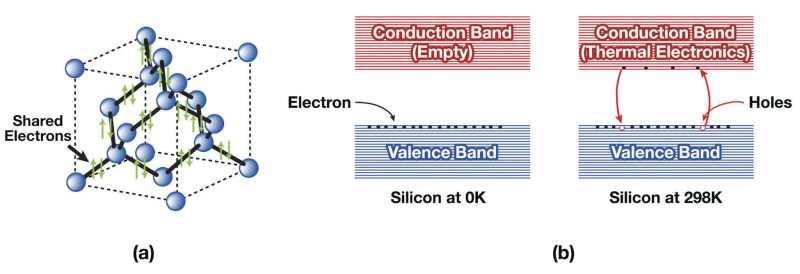
Illustrative Image (Source: Google Search)
The production of silicon-based conductive components typically involves several key stages, each crucial to achieving the desired electrical performance and material integrity.
Robust quality assurance is vital to guarantee that silicon conductive products meet stringent performance and safety requirements demanded by international markets.
For buyers in emerging and established markets, ensuring supplier quality is paramount to mitigate risks and ensure compliance.
In summary, B2B buyers sourcing silicon conductive materials must engage deeply with both the manufacturing nuances and quality assurance frameworks. By understanding material preparation, fabrication techniques, and rigorous QC practices aligned with international standards, buyers can confidently select suppliers that deliver reliable, compliant silicon components tailored to their regional and industry-specific requirements.
Understanding the cost and pricing dynamics of sourcing silicon materials for electrical conductivity applications is essential for international B2B buyers aiming to optimize procurement strategies and ensure competitive positioning. This section breaks down the key cost components, pricing influencers, and practical buyer tips, with a focus on markets in Africa, South America, the Middle East, and Europe.
Raw Materials
The primary cost driver is the raw silicon itself, often purified to different grades depending on application needs. Prices fluctuate based on global silicon supply-demand, purity levels, and the inclusion of doping elements that enhance conductivity.
Labor Costs
Labor expenses vary significantly by region and impact manufacturing and processing costs. Regions with advanced semiconductor industries (e.g., Europe) may have higher labor costs compared to emerging manufacturing hubs, but often benefit from higher efficiency and quality.
Manufacturing Overhead
This includes factory utilities, depreciation of equipment, and indirect labor. Overhead costs are influenced by the scale of production and technology sophistication used in silicon wafer slicing, doping, and packaging.
Tooling and Equipment
High precision tooling is required for processing silicon to meet electrical specifications. Initial tooling investments may be amortized over large volumes but can be a significant upfront cost, especially for customized specifications.
Quality Control (QC)
Rigorous QC processes ensure conformity with electrical and physical standards, which is critical for reliability in B2B applications. QC costs may include testing equipment, certification fees, and labor.
Logistics and Shipping
Silicon wafers and related materials require careful handling to avoid contamination or damage. Logistics costs are affected by shipping modes, distances, customs duties, and regional infrastructure—factors particularly relevant for buyers in Africa, South America, and the Middle East.
Supplier Margin
Margins vary depending on supplier positioning, exclusivity of technology, and market demand. Negotiating margins is often possible in high-volume contracts or long-term partnerships.
Order Volume and Minimum Order Quantities (MOQ)
Larger order volumes usually attract volume discounts, while smaller orders may incur premium pricing. Buyers should balance MOQ requirements with inventory capabilities.
Technical Specifications and Customization
Custom doping levels, wafer thickness, and surface treatments can increase costs. Standard specifications typically offer better pricing.
Material Grade and Purity
Higher purity silicon for advanced conductivity commands higher prices. Certifications such as ISO or RoHS compliance can also impact costs but are essential for quality assurance.
Supplier Reputation and Location
Suppliers based in technologically advanced countries may offer superior quality but at higher prices. Conversely, emerging market suppliers might provide cost advantages but require diligent vetting.
Incoterms and Payment Terms
Shipping terms (e.g., FOB, CIF) influence who bears shipping and insurance costs. Favorable payment terms can improve cash flow and reduce financing costs.
Engage in Strategic Negotiations
Leverage volume commitments and long-term agreements to negotiate better pricing and favorable payment terms. For buyers in regions with developing supply chains (Africa, South America), establishing relationships with reliable suppliers is key.
Evaluate Total Cost of Ownership (TCO)
Consider all costs beyond unit price, including logistics, tariffs, quality failures, and lead times. For example, sourcing from Europe may have higher upfront costs but reduce risks and delays.
Verify Certifications and Compliance
Ensuring materials meet international standards avoids costly rejections and delays. For buyers in regulated markets like the EU (Italy) or export-driven economies (Argentina), compliance is non-negotiable.
Factor in Currency Fluctuations and Local Taxes
Currency volatility can impact landed costs significantly. Hedging strategies or multi-currency contracts may mitigate risks.
Plan for Logistics Complexity
Infrastructure challenges in some African and Middle Eastern regions necessitate robust logistics planning. Use reputable freight forwarders and consider insurance for high-value shipments.
Prices for silicon materials with conductive properties vary widely depending on grade, volume, and market conditions. The insights provided herein serve as a guide to understanding cost drivers and pricing factors but should not be used as definitive price quotations. Buyers are advised to request detailed quotations and conduct supplier audits to obtain precise pricing tailored to their specific sourcing requirements.
By comprehensively analyzing these cost and pricing factors, B2B buyers can make informed decisions that balance quality, cost-efficiency, and supply chain resilience in sourcing silicon for electrical conductivity applications.
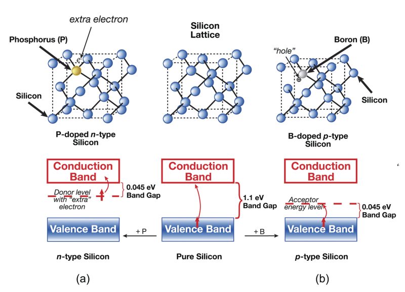
When sourcing silicon materials designed to conduct electricity, understanding key technical specifications is essential for ensuring performance, reliability, and cost-efficiency in your applications. Below are the most crucial properties B2B buyers should evaluate:
Material Grade
Silicon is available in various grades such as metallurgical grade, solar grade, and electronic grade. For electrical conductivity, electronic grade silicon is preferred due to its high purity (99.9999% or higher), which ensures minimal electrical resistance and superior performance in semiconductor devices. Selecting the right grade directly impacts device efficiency and lifespan.
Resistivity (Ω·cm)
Resistivity measures how strongly silicon opposes the flow of electric current. Lower resistivity indicates better conductivity. Depending on the application, resistivity can range from a few milliohm-centimeters for highly conductive silicon to several ohm-centimeters for less conductive types. Buyers should specify resistivity to match circuit requirements and avoid signal loss.
Doping Concentration
Silicon’s conductivity is enhanced by doping it with impurities like phosphorus (n-type) or boron (p-type). The doping concentration (atoms per cm³) determines electrical characteristics such as carrier concentration and mobility. Precise doping levels are vital for consistent electrical behavior in semiconductors and sensors.
Wafer Thickness and Size
For silicon wafers used in electronics, thickness (typically 200-800 microns) and diameter (100 mm to 300 mm) affect mechanical strength and compatibility with manufacturing equipment. Uniformity in wafer size and thickness reduces defects and improves yield, which is critical for large-scale B2B procurement.
Surface Finish and Flatness
A polished surface with controlled flatness ensures optimal contact and minimal resistance in electrical components. Specifications like surface roughness (measured in angstroms) and total thickness variation (TTV) are important for buyers targeting high-frequency or precision devices.
Thermal Conductivity
Although primarily an electrical conductor, silicon’s ability to dissipate heat impacts device reliability. Thermal conductivity values help buyers assess how well the material can manage operational heat, especially in power electronics and photovoltaic modules.
Understanding trade terms and industry jargon helps international buyers navigate contracts, negotiations, and logistics efficiently:
OEM (Original Equipment Manufacturer)
Refers to companies that produce parts or components used in another company’s end products. When buying silicon, knowing if the supplier is an OEM or a distributor affects pricing, customization options, and warranty terms.
MOQ (Minimum Order Quantity)
The smallest quantity a supplier is willing to sell. MOQs influence inventory planning and cost management, especially for buyers in emerging markets or those testing new silicon materials.
RFQ (Request for Quotation)
A formal document sent to suppliers asking for price, availability, and terms. Crafting a detailed RFQ including required silicon specifications helps buyers receive accurate quotes and compare offers transparently.
Incoterms (International Commercial Terms)
Standardized trade terms defining responsibilities for shipping, insurance, and customs between buyer and seller. Common Incoterms include FOB (Free on Board) and CIF (Cost, Insurance, and Freight). Selecting appropriate Incoterms reduces misunderstandings and controls logistics costs.
Lead Time
The period between placing an order and receiving the goods. Silicon supply chains can be affected by production complexity and global demand; understanding lead times helps avoid project delays.
Traceability
The ability to track silicon material back through its production and supply chain. Traceability is critical for quality assurance and compliance with international standards, especially in regulated industries like automotive and aerospace.
By prioritizing these technical properties and mastering key trade terms, B2B buyers from diverse regions—including Africa, South America, the Middle East, and Europe—can make informed purchasing decisions that align with their operational needs and market requirements. This approach minimizes risk, optimizes costs, and fosters strong supplier relationships in the global silicon market.
The global market for silicon-based electrical conductors is experiencing dynamic growth fueled by expanding applications in electronics, renewable energy, and automotive sectors. Silicon's unique semiconducting properties make it indispensable for components such as photovoltaic cells, power semiconductors, and integrated circuits. For international B2B buyers, particularly in Africa, South America, the Middle East, and Europe, understanding regional demand drivers and supply chain nuances is crucial for strategic sourcing.
Key market drivers include the accelerating adoption of solar energy technologies, increasing electrification in emerging markets, and advancements in silicon wafer manufacturing that enhance conductivity and efficiency. Europe, notably Italy, is focusing on integrating silicon-based components into smart grids and electric vehicles, while South American markets like Argentina are leveraging silicon for expanding renewable infrastructure. In the Middle East and Africa, growing investments in energy diversification and industrial automation are propelling demand.
Emerging sourcing trends emphasize supplier consolidation and vertical integration to ensure material quality and reduce lead times. Buyers are increasingly seeking partnerships with manufacturers who offer cutting-edge silicon purity levels and custom doping processes to meet specialized conductivity requirements. Additionally, digital procurement platforms and blockchain technologies are gaining traction to enhance transparency and traceability in sourcing.
Market dynamics reveal a shift towards localized production hubs to mitigate risks associated with global logistics disruptions. African and South American buyers are exploring regional suppliers to balance cost efficiency with reliability, while European companies prioritize compliance with stringent quality and environmental standards. Understanding these trends allows B2B buyers to optimize their procurement strategies and foster resilient supply chains.
Sustainability considerations are becoming a pivotal factor in sourcing silicon conductors, driven by both regulatory pressures and corporate responsibility commitments. The silicon production process, particularly refining and doping, is energy-intensive and can generate significant environmental footprints if not managed responsibly.
B2B buyers must prioritize ethical sourcing to ensure their supply chains minimize adverse environmental and social impacts. This involves selecting suppliers who adhere to internationally recognized standards such as ISO 14001 for environmental management and who demonstrate transparency in labor practices. Certifications like the Responsible Minerals Initiative (RMI) or equivalent local certifications can provide assurance against sourcing from conflict-affected or high-risk areas.
Green materials and processes are gaining prominence, with innovations such as low-carbon silicon manufacturing using renewable energy sources and closed-loop water recycling systems. Buyers should evaluate suppliers based on their carbon intensity, waste management protocols, and commitment to circular economy principles, such as silicon recycling from end-of-life electronic components.
By integrating sustainability criteria into supplier evaluation and contract negotiation, international buyers can reduce regulatory risks, enhance brand reputation, and align with the growing demand for environmentally responsible electronics. This approach is particularly critical for buyers in Europe, where regulatory frameworks like the EU Green Deal impose stringent environmental compliance, but is increasingly relevant across all target regions.
Silicon’s role as a conductor has evolved significantly since its mid-20th century emergence as a semiconductor material. Initially prized for its abundant availability and semiconducting properties, silicon replaced earlier materials like germanium due to its superior thermal stability and cost efficiency. The development of the silicon wafer revolutionized the electronics industry, enabling mass production of integrated circuits and solar cells.
For B2B buyers, understanding this evolution underscores the importance of silicon purity and manufacturing precision in achieving optimal electrical performance. Advances in crystal growth techniques and doping technologies have progressively enhanced conductivity and reliability, shaping the current supply landscape. This historical trajectory also highlights the sector’s ongoing innovation, informing buyer decisions around technology adoption and supplier capabilities.
How can I effectively vet suppliers of silicon conduct electricity for international B2B purchases?
Conduct thorough due diligence by verifying the supplier’s business licenses, certifications (such as ISO or industry-specific standards), and financial stability. Request references and check their track record in supplying silicon materials globally, particularly to regions like Africa, South America, the Middle East, and Europe. Utilize third-party audits or inspection services to assess production facilities and quality control processes. Engaging with trade associations and participating in industry exhibitions can also help identify reputable suppliers with proven export experience.
Is customization of silicon conduct electricity products typically available for international buyers?
Yes, many suppliers offer customization options tailored to specific electrical conductivity requirements, purity levels, wafer sizes, or packaging preferences. It’s important to communicate your technical specifications clearly and confirm the supplier’s capability to meet these requirements. Customization may affect lead times and pricing, so negotiate terms upfront. For buyers in diverse markets like Italy or Argentina, ensure that the supplier understands local standards and application needs to optimize product performance.
What are common Minimum Order Quantities (MOQs) and lead times for silicon conduct electricity shipments to Africa, South America, or the Middle East?
MOQs vary widely depending on the supplier’s production scale and the complexity of the silicon product, often ranging from small batch orders of a few kilograms to several tons. Lead times typically range from 4 to 12 weeks, factoring in manufacturing, quality checks, and international shipping. Buyers should request detailed production schedules and negotiate flexible MOQs if entering new markets. Early planning and clear communication help mitigate delays, especially when shipping to regions with complex customs procedures.
What payment terms are advisable when sourcing silicon conduct electricity internationally?
Secure payment methods such as Letters of Credit (LC) or escrow services are recommended to protect both buyer and supplier interests. Partial upfront payments combined with balance payments upon delivery or after quality inspection can balance risk. For established partnerships, net payment terms (e.g., 30-60 days) may be negotiated. Always ensure payment terms comply with your country’s foreign exchange regulations and consider currency fluctuation risks, especially in emerging markets like Africa or South America.
Illustrative Image (Source: Google Search)
Which quality assurance certifications should I require from silicon conduct electricity suppliers?
Request suppliers to provide internationally recognized certifications such as ISO 9001 for quality management and industry-specific standards like SEMI (Semiconductor Equipment and Materials International) certifications. Additionally, ask for material safety data sheets (MSDS), test reports verifying electrical conductivity and purity, and compliance with RoHS (Restriction of Hazardous Substances) if applicable. These documents ensure consistent product quality and regulatory compliance across diverse markets.
What are the best logistics practices for shipping silicon conduct electricity to international destinations?
Silicon products require careful handling to avoid contamination or damage. Choose suppliers and freight forwarders experienced with sensitive electronic materials. Opt for reliable shipping methods (air freight for urgent orders; sea freight for bulk shipments) with clear tracking capabilities. Understand customs requirements and tariffs in target markets like the Middle East or Europe, and prepare all documentation meticulously. Establish contingency plans for delays and consider insurance to mitigate transit risks.
How should I handle disputes or quality issues with overseas silicon conduct electricity suppliers?
Establish clear contractual terms covering product specifications, inspection rights, dispute resolution mechanisms, and penalties for non-compliance. Engage third-party inspection agencies for independent verification before shipment. In case of disputes, initiate dialogue promptly and document all communications. Arbitration clauses specifying neutral venues or internationally recognized bodies (e.g., ICC) provide structured resolution pathways. Building long-term relationships with transparent communication reduces conflict risks.
Are there regional considerations for buying silicon conduct electricity in markets like Italy, Argentina, or the Middle East?
Yes, regional market dynamics affect sourcing strategies. For example, European buyers such as in Italy may prioritize suppliers with strong environmental compliance and advanced certification. South American buyers in Argentina should consider import tariffs and logistics infrastructure challenges. Middle Eastern buyers often seek suppliers familiar with local regulations and capable of providing after-sales technical support. Understanding these nuances allows tailored negotiation and smoother supply chain management.
The information provided in this guide, including content regarding manufacturers, technical specifications, and market analysis, is for informational and educational purposes only. It does not constitute professional procurement advice, financial advice, or legal advice.
While we have made every effort to ensure the accuracy and timeliness of the information, we are not responsible for any errors, omissions, or outdated information. Market conditions, company details, and technical standards are subject to change.
B2B buyers must conduct their own independent and thorough due diligence before making any purchasing decisions. This includes contacting suppliers directly, verifying certifications, requesting samples, and seeking professional consultation. The risk of relying on any information in this guide is borne solely by the reader.
Strategic sourcing of silicon for electrical conductivity applications remains a cornerstone for businesses aiming to optimize performance and cost-efficiency in an increasingly competitive global market. For B2B buyers across Africa, South America, the Middle East, and Europe, understanding the nuances of silicon’s electrical properties, supply chain dynamics, and quality specifications is essential to secure reliable and innovative materials.
Key takeaways include the importance of partnering with suppliers who demonstrate transparency, technical expertise, and compliance with international standards. Emphasizing sustainability and supply chain resilience can mitigate risks associated with geopolitical shifts and raw material scarcity. Leveraging regional trade agreements and local market insights, particularly in emerging economies like Argentina and Italy, can unlock cost advantages and foster long-term collaboration.
Looking ahead, investing in strategic sourcing will empower businesses to harness silicon’s full potential in cutting-edge electronics, renewable energy, and smart technologies. International buyers are encouraged to deepen supplier relationships, explore diversified sourcing channels, and stay informed on technological advancements. By doing so, they will not only enhance their competitive edge but also contribute to a more sustainable and interconnected global supply ecosystem.
Illustrative Image (Source: Google Search)
Tags: Black Silicon Carbide, White Fused Alumina, Brown Fused Alumina, Pink Fused Alumina, Black Fused Alumina