Silicon substrates form the foundational backbone of modern electronics, powering everything from semiconductors and integrated circuits to advanced photovoltaic cells. For international B2B buyers—especially those operating in dynamic markets across Africa, South America, the Middle East, and Europe—understanding the complexities of silicon substrate sourcing is crucial to maintaining competitive advantage and ensuring product excellence.
This guide offers an authoritative roadmap through the intricate global market of silicon substrates. It comprehensively covers key areas including:
By consolidating this critical information, the guide empowers B2B buyers in countries such as Nigeria, Brazil, the UAE, and France to make informed, strategic sourcing decisions. Leveraging these insights will help businesses optimize supply reliability, reduce costs, and enhance product quality in a rapidly evolving technological landscape.
| Type Name | Key Distinguishing Features | Primary B2B Applications | Brief Pros & Cons for Buyers |
|---|---|---|---|
| Monocrystalline Silicon (Mono-Si) | Single crystal structure, uniform lattice, high purity | High-performance semiconductors, IC wafers | Pros: Superior electronic properties, high efficiency; Cons: Higher cost, complex manufacturing |
| Polycrystalline Silicon (Poly-Si) | Multiple small silicon crystals, less uniform structure | Solar cells, sensors, lower-end semiconductor devices | Pros: Lower cost, easier production; Cons: Lower efficiency, more defects |
| Amorphous Silicon (a-Si) | Non-crystalline, disordered atomic structure | Thin-film solar panels, LCD displays | Pros: Flexible substrates, low-temperature processing; Cons: Lower carrier mobility, less stable |
| Silicon-on-Insulator (SOI) | Thin silicon layer on an insulating substrate (e.g., silicon dioxide) | High-speed, low-power electronics, RF applications | Pros: Reduced parasitic capacitance, improved performance; Cons: Higher substrate cost, complex fabrication |
| Epitaxial Silicon (Epi-Si) | Thin, high-quality silicon layer grown on a silicon wafer | Advanced microelectronics, power devices | Pros: Tailored electrical properties, improved device performance; Cons: Expensive, requires precise control |
Monocrystalline silicon substrates feature a continuous and uniform crystal lattice, making them ideal for high-precision semiconductor manufacturing. Their high purity and structural uniformity enable excellent electrical performance, critical for integrated circuits and advanced microchips. Buyers from industries such as electronics manufacturing in Europe and the Middle East often prioritize Mono-Si for its reliability despite its higher cost. When sourcing, consider wafer size, resistivity, and crystal orientation to match device requirements.
Polycrystalline silicon consists of numerous small silicon crystals, resulting in a less uniform structure than Mono-Si. It is widely used in solar photovoltaic panels and lower-cost semiconductor devices, favored for its cost-effectiveness. Buyers in emerging African and South American markets appreciate Poly-Si for balancing performance and budget constraints. Key purchasing factors include grain size, purity levels, and surface finish, which influence efficiency and yield.
Amorphous silicon lacks a defined crystal structure, offering flexibility and ease of deposition on various substrates, including glass and plastic. This makes it well-suited for thin-film solar panels and display technologies. B2B buyers targeting flexible electronics or cost-sensitive solar applications in regions like Nigeria or Brazil should focus on a-Si’s trade-offs between lower electronic mobility and manufacturing versatility. Important considerations include film thickness, deposition method, and stability under operational conditions.
SOI substrates incorporate a thin silicon layer separated from the bulk substrate by an insulating layer, typically silicon dioxide. This design reduces parasitic capacitance, improving device speed and lowering power consumption, which is crucial for RF and high-speed digital circuits. Buyers in Europe and the Middle East engaged in advanced electronics manufacturing often seek SOI for performance gains. Key purchasing parameters include the thickness of silicon and insulator layers and wafer quality.
Epitaxial silicon involves growing a high-quality silicon layer atop a silicon wafer, allowing customization of electrical properties to enhance device performance, particularly in power electronics and microprocessors. This substrate type demands precise process control and is generally more expensive. B2B buyers should evaluate epitaxial layer thickness, doping concentration, and defect density to ensure compatibility with their semiconductor fabrication processes. This type is favored in high-tech markets across Europe and the Middle East.
Related Video: Silicon Wafer Production
| Industry/Sector | Specific Application of Silicon Substrate | Value/Benefit for the Business | Key Sourcing Considerations for this Application |
|---|---|---|---|
| Semiconductor | Fabrication of integrated circuits and microchips | Enables high-performance, miniaturized electronic components | Purity, wafer size uniformity, defect density, and supplier reliability |
| Photovoltaics | Base material for solar cells | Improves solar conversion efficiency and durability | Crystalline quality, surface flatness, and cost-effectiveness |
| MEMS (Microelectromechanical Systems) | Substrate for sensors and actuators | Facilitates compact, precise sensing devices for industrial use | Mechanical strength, thermal stability, and compatibility with MEMS processes |
| LED Manufacturing | Substrate for LED chips | Enhances light emission efficiency and device longevity | Thermal conductivity, defect-free surface, and cost efficiency |
| Power Electronics | Substrate for power semiconductor devices | Supports high voltage and current handling with improved reliability | Resistivity control, thermal management capabilities, and quality certification |
Silicon substrates are foundational in the semiconductor industry, where they serve as the base material for fabricating integrated circuits and microchips. For international buyers in regions like Africa or South America, sourcing high-purity silicon wafers with minimal defects is critical to ensure device performance and yield. Buyers should prioritize suppliers that provide consistent wafer uniformity and reliable logistics to mitigate the risks of delays and quality issues.
In the photovoltaic sector, silicon substrates form the core of solar cells. The crystalline quality and surface flatness directly impact solar energy conversion efficiency, a vital consideration for energy companies in the Middle East or Europe seeking to optimize renewable energy projects. Cost-effective sourcing combined with high-quality crystalline substrates can significantly improve the return on investment for solar power installations.
For MEMS applications, silicon substrates are used to build micro-scale sensors and actuators essential in automotive, healthcare, and industrial automation markets. Buyers must ensure the substrates have excellent mechanical strength and thermal stability to withstand processing and operational stresses. Regions such as Nigeria or France may require sourcing partners that can tailor substrate specifications to unique MEMS device requirements and comply with international quality standards.
In LED manufacturing, silicon substrates enhance the performance of LED chips by improving light emission and thermal management. This is especially relevant for lighting manufacturers and electronics firms in Europe and the Middle East aiming to produce energy-efficient and durable lighting solutions. Key sourcing factors include thermal conductivity of the substrate and the absence of surface defects that could impair LED function.
Finally, in power electronics, silicon substrates are critical for devices handling high voltages and currents, such as power transistors and diodes. Buyers from industrial sectors in South America or Africa should focus on substrates with controlled resistivity and superior thermal management to ensure device reliability and longevity. Certification of quality and adherence to industry standards are essential considerations for international procurement in this domain.
Key Properties:
Monocrystalline silicon substrates feature a uniform crystal lattice, offering excellent electrical properties, high thermal conductivity, and superior mechanical strength. They typically withstand temperatures up to 1400°C and exhibit good corrosion resistance in standard semiconductor processing environments.
Pros & Cons:
- Pros: High purity and uniformity ensure excellent device performance and reliability. Ideal for high-precision electronics and photovoltaic applications.
- Cons: Manufacturing complexity is high, leading to elevated costs. Fragility during handling requires careful logistics and packaging.
- Impact on Application: Best suited for integrated circuits, MEMS devices, and high-efficiency solar cells where defect minimization is critical.
International Buyer Considerations:
Buyers from regions like Europe (e.g., France) benefit from well-established supply chains and compliance with international standards such as ASTM F121-13 and IEC 60216. In emerging markets like Nigeria and parts of South America, ensuring supplier certification and quality control is vital due to variability in local infrastructure. Import tariffs and customs duties may also impact cost-effectiveness.
Key Properties:
Polycrystalline silicon substrates consist of multiple small silicon crystals, offering moderate electrical performance and lower thermal conductivity compared to monocrystalline types. They tolerate similar temperature ranges but have slightly reduced mechanical strength.
Pros & Cons:
- Pros: Lower production costs and simpler manufacturing processes make this material attractive for large-scale applications. More tolerant to defects and easier to produce in larger wafers.
- Cons: Reduced efficiency in electronic and photovoltaic devices due to grain boundaries. Less uniformity can affect device consistency.
- Impact on Application: Commonly used in cost-sensitive solar panels and certain sensor applications where absolute performance is less critical.
International Buyer Considerations:
For buyers in the Middle East and Africa, polycrystalline silicon is often preferred due to cost constraints and the growing solar energy market. Compliance with IEC 61215 and IEC 61730 standards is essential for export and installation in these regions. Buyers should verify the material’s origin and quality certifications to avoid substandard imports.
Key Properties:
SOI substrates consist of a thin silicon layer separated from the bulk substrate by an insulating oxide layer. This structure offers reduced parasitic capacitance, improved thermal isolation, and enhanced radiation hardness.
Pros & Cons:
- Pros: Superior performance in high-speed and low-power applications. Enhanced device isolation improves yield and reliability.
- Cons: Higher manufacturing complexity and cost. Limited wafer sizes and availability can affect supply chain flexibility.
- Impact on Application: Ideal for RF devices, power management ICs, and aerospace electronics requiring radiation resistance.
International Buyer Considerations:
European buyers often demand SOI substrates for advanced semiconductor manufacturing, adhering to strict DIN EN ISO standards. In South America and the Middle East, the adoption of SOI technology is growing but may be limited by infrastructure and cost. Buyers should engage with suppliers offering robust logistics and after-sales support to mitigate supply risks.
Key Properties:
Amorphous silicon lacks a long-range crystal structure, resulting in lower electrical conductivity and mechanical strength but offering flexibility in deposition over large areas and on flexible substrates.
Pros & Cons:
- Pros: Cost-effective for thin-film applications and flexible electronics. Simple deposition processes compatible with large-area substrates.
- Cons: Poor charge carrier mobility limits use in high-performance devices. Stability and durability concerns under prolonged stress.
- Impact on Application: Widely used in thin-film solar cells, flexible displays, and sensor arrays where cost and form factor outweigh performance.
International Buyer Considerations:
Buyers in Africa and South America can leverage amorphous silicon for emerging markets focusing on affordable solar solutions and flexible electronics. Compliance with IEC 61646 and IEC 61730 standards ensures product reliability. Due to lower mechanical robustness, buyers must ensure proper handling and storage during transport.
| Material | Typical Use Case for silicon substrate | Key Advantage | Key Disadvantage/Limitation | Relative Cost (Low/Med/High) |
|---|---|---|---|---|
| Monocrystalline Silicon | High-performance semiconductors, photovoltaics | Superior electrical properties and uniformity | High cost and fragile handling requirements | High |
| Polycrystalline Silicon | Cost-sensitive solar panels and sensors | Lower cost and easier manufacturing | Reduced efficiency due to grain boundaries | Low |
| Silicon-on-Insulator (SOI) | RF devices, aerospace electronics, power ICs | Enhanced device isolation and radiation hardness | Complex manufacturing and limited availability | High |
| Amorphous Silicon | Thin-film solar cells, flexible electronics | Cost-effective and flexible substrate options | Lower electrical performance and durability | Low |
This guide equips international B2B buyers with a strategic understanding of silicon substrate materials, tailored to diverse regional needs and industrial standards. By aligning material properties with application demands and regional considerations, buyers can optimize procurement decisions for performance, cost, and compliance.
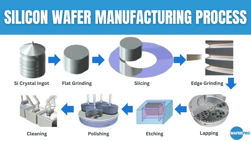
The production of silicon substrates, a critical component in semiconductor devices, involves a series of highly controlled stages designed to ensure purity, structural integrity, and optimal electrical properties. Understanding these stages enables B2B buyers, especially from regions like Africa, South America, the Middle East, and Europe, to assess supplier capabilities and product suitability.
The process begins with the procurement and purification of raw silicon, typically derived from quartz sand. The silicon is refined through chemical vapor deposition and zone refining to achieve semiconductor-grade purity (often 99.9999% or higher). This high-purity silicon is essential for minimizing defects that could impact device performance.
The purified silicon is melted and formed into large single crystals using methods such as the Czochralski (CZ) process or the Float Zone (FZ) technique. These methods produce cylindrical ingots with uniform crystal orientation and minimal impurities. The ingots are then sliced into thin wafers using diamond wire saws, with thickness and diameter specifications tailored to end-use requirements.
Following slicing, wafers undergo grinding and lapping to remove surface damage and achieve flatness. Chemical-mechanical polishing (CMP) is applied to create an ultra-smooth, defect-free surface critical for subsequent device fabrication. Surface cleaning processes remove contaminants and particles, ensuring high surface quality.
In some cases, silicon substrates may be assembled with additional layers or components, such as epitaxial layers or insulating films, depending on the application. This stage involves thin-film deposition, doping, and annealing steps, requiring precise control to maintain substrate integrity.
The final stage includes marking, packaging, and protective coating application to safeguard the wafers during transport. Careful handling and packaging standards prevent contamination and mechanical damage.
Quality control is paramount in silicon substrate production due to the stringent requirements of semiconductor applications. B2B buyers must prioritize suppliers with robust QA/QC systems aligned with international and industry-specific standards.
For international B2B buyers, especially those from emerging markets and regions with diverse regulatory environments, verifying supplier QC processes is critical to mitigate risks.
B2B buyers from diverse regions face unique challenges and opportunities when sourcing silicon substrates internationally.
By comprehensively understanding the manufacturing steps and quality assurance processes for silicon substrates, international B2B buyers can make informed sourcing decisions, ensure product reliability, and foster long-term supplier partnerships tailored to their regional market needs.
When sourcing silicon substrates, international B2B buyers must carefully evaluate the cost structure to make informed purchasing decisions. The primary cost components typically include:
Several factors influence pricing dynamics beyond basic cost elements:
For buyers in Nigeria, Brazil, the Middle East, France, and other regions, adopting strategic procurement practices can optimize costs and reduce risk:
Prices for silicon substrates vary widely depending on grade, size, customization, and market conditions. The figures and factors discussed here serve as general guidance and should not replace direct supplier quotations. Buyers are encouraged to conduct detailed cost analyses and engage multiple suppliers to secure competitive and transparent pricing.
By understanding the detailed cost structure and pricing influencers, international B2B buyers can strategically navigate the silicon substrate market. This insight empowers procurement teams to negotiate effectively, optimize their investment, and ensure supply chain resilience across diverse global regions.
Understanding the critical technical specifications of silicon substrates is essential for international B2B buyers to make informed procurement decisions that align with their manufacturing needs and quality standards.
Material Grade (Purity Level)
Silicon substrates vary in purity, typically measured in terms of electronic-grade silicon (EGS) with purity levels exceeding 99.9999%. Higher purity ensures better electrical performance and fewer defects in semiconductor applications. For buyers in sectors like electronics manufacturing, selecting the correct purity level is crucial to achieve product reliability.
Wafer Diameter and Thickness
Common wafer diameters range from 100 mm to 300 mm, with thicknesses tailored to specific process requirements. Larger diameters generally allow higher production efficiency but may come at increased cost. Buyers should confirm compatibility with their fabrication equipment and production scale to optimize cost and yield.
Crystallographic Orientation
The crystal orientation, such as <100> or <111>, affects the mechanical strength and electrical characteristics of the substrate. This property influences etching processes and device performance. Knowing the orientation helps buyers ensure substrate suitability for their intended semiconductor device designs.
Surface Flatness and Roughness
Surface flatness, often defined by Total Thickness Variation (TTV), and surface roughness impact layer uniformity and subsequent device fabrication quality. Tight flatness tolerances reduce defects during photolithography and thin-film deposition. Buyers should specify these parameters to meet high-precision manufacturing standards.
Doping Type and Concentration
Silicon substrates can be doped with elements like boron (p-type) or phosphorus (n-type) to modify electrical properties. The doping concentration affects conductivity and device behavior. Clear specifications on doping allow buyers to tailor substrates to their circuit requirements.
Defect Density
Refers to the number of crystallographic defects per unit area, affecting yield and performance. Lower defect densities are preferred for high-end semiconductor devices. Buyers targeting advanced electronics should prioritize substrates with minimal defects.
Navigating B2B transactions requires familiarity with key industry terms that facilitate clear communication and efficient purchasing processes.
OEM (Original Equipment Manufacturer)
Refers to companies that produce components or products used in another company's end products. Buyers often source silicon substrates from OEMs to ensure quality and reliability consistent with original design specifications.
MOQ (Minimum Order Quantity)
The smallest quantity of silicon substrates a supplier is willing to sell per order. Understanding MOQ is vital for buyers in emerging markets or smaller operations (e.g., in Nigeria or South America) to manage inventory costs and cash flow effectively.
RFQ (Request for Quotation)
A formal document sent to suppliers asking for pricing, lead times, and terms for silicon substrates. RFQs are essential for obtaining competitive bids and clarifying technical requirements before purchase.
Incoterms (International Commercial Terms)
Standardized trade terms defining responsibilities for shipping, insurance, customs clearance, and delivery between buyers and sellers. Common Incoterms include FOB (Free On Board) and CIF (Cost, Insurance, and Freight). Buyers should negotiate Incoterms carefully to control logistics costs and risks, particularly when importing to regions like the Middle East or Europe.
Yield
The percentage of usable substrates or wafers after processing, reflecting manufacturing efficiency. High yield substrates reduce production costs and waste, a key consideration for cost-sensitive buyers.
Traceability
The ability to track the origin and processing history of silicon substrates. Traceability ensures quality control and compliance with international standards, important for buyers aiming for certifications or entering regulated markets.
By focusing on these technical properties and mastering the relevant trade terminology, B2B buyers across Africa, South America, the Middle East, and Europe can optimize their silicon substrate procurement strategies. This approach helps secure high-quality materials, negotiate better terms, and align supply chain operations with their manufacturing goals.
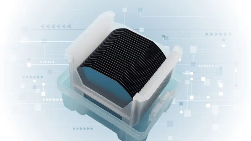
Illustrative Image (Source: Google Search)
The global silicon substrate market is experiencing robust growth driven by the expanding semiconductor, solar energy, and electronics industries. Key demand centers include advanced economies in Europe (notably France and Germany) and emerging markets across Africa, South America, and the Middle East, where digital transformation and renewable energy adoption are accelerating. Buyers from regions like Nigeria and Brazil are increasingly sourcing high-quality silicon substrates to support local manufacturing and technology development, reflecting a broader trend of regional supply chain diversification.
Market dynamics are shaped by technological advancements such as the transition to larger wafer sizes (200mm to 300mm and beyond) and the rise of new materials tailored for high-performance computing, 5G infrastructure, and electric vehicles. Suppliers are investing heavily in precision polishing and defect reduction technologies, which are critical for meeting stringent semiconductor fabrication requirements. International buyers should note a growing emphasis on supply chain resilience, with many companies seeking multi-region sourcing strategies to mitigate geopolitical risks and material shortages.
Sourcing trends emphasize strategic partnerships and long-term contracts, particularly for buyers in emerging markets aiming to secure stable silicon substrate supplies amidst global volatility. Digital platforms and B2B marketplaces are increasingly facilitating direct engagement between manufacturers and buyers, enabling better transparency and customization. Additionally, the integration of AI-driven quality control and predictive analytics in manufacturing is enhancing product consistency and delivery reliability.
Sustainability has become a critical consideration in the silicon substrate sector, driven by growing regulatory pressures and corporate responsibility commitments worldwide. The production of silicon wafers involves energy-intensive processes and chemical treatments, which contribute to carbon emissions and waste generation. B2B buyers, especially those in Europe and progressive markets in the Middle East, are prioritizing suppliers that demonstrate environmentally responsible manufacturing practices and adherence to international environmental standards.
Ethical sourcing extends beyond environmental impact to encompass labor practices and transparent supply chains. Buyers from regions such as Africa and South America are increasingly scrutinizing supplier certifications, including ISO 14001 (Environmental Management), RoHS (Restriction of Hazardous Substances), and conflict-free sourcing declarations. These certifications not only mitigate reputational risks but also align with global sustainability goals.
The emergence of “green silicon” initiatives, involving the use of recycled silicon and renewable energy-powered manufacturing plants, offers new opportunities for buyers committed to reducing their carbon footprint. Engaging with suppliers who invest in circular economy principles and clean energy can enhance compliance with evolving sustainability mandates and appeal to end customers demanding greener products.
The silicon substrate industry has evolved significantly since its inception in the mid-20th century, paralleling the rise of the semiconductor revolution. Early silicon wafers were relatively small and produced with limited precision, restricting their use to basic electronic devices. Over the decades, advancements in crystal growth methods (such as the Czochralski process) and wafer fabrication techniques have enabled larger, defect-free substrates essential for modern integrated circuits.
Illustrative Image (Source: Google Search)
This evolution has been driven by the relentless pursuit of smaller, faster, and more energy-efficient chips, compelling substrate manufacturers to innovate continuously. Today, silicon substrates are foundational to cutting-edge technologies including microprocessors, solar cells, and MEMS devices. For international B2B buyers, understanding this historical context underscores the importance of selecting suppliers with proven expertise and technological leadership to meet future market demands.
Illustrative Image (Source: Google Search)
How can I effectively vet silicon substrate suppliers internationally, especially from regions like Africa or South America?
To vet suppliers, start by verifying their business licenses and certifications such as ISO 9001 or industry-specific quality accreditations. Request product samples to assess quality firsthand. Check for references or client testimonials, particularly from buyers in your region or industry. Utilize third-party inspection services or local agents to audit production facilities. Digital platforms like Alibaba or global trade directories offer supplier ratings, but always conduct independent due diligence. Establish clear communication channels and confirm their export experience to ensure smooth cross-border transactions.
Is customization of silicon substrates possible, and what should buyers from the Middle East or Europe consider?
Many suppliers offer customization in wafer size, thickness, resistivity, and surface finish to meet specific application needs. Buyers should clearly specify technical parameters and tolerances upfront. Custom orders often have higher minimum order quantities (MOQs) and longer lead times. Verify the supplier’s capability to deliver consistent quality in customized products through samples and technical datasheets. Also, consider compliance with regional standards such as RoHS or REACH when ordering for Europe or the Middle East markets.
What are typical minimum order quantities (MOQs) and lead times for silicon substrates, and how can buyers negotiate these terms?
MOQs vary widely, commonly ranging from a few hundred to several thousand wafers depending on customization and supplier scale. Standard products usually have shorter lead times (2-4 weeks), while custom orders may require 6-12 weeks. Buyers should communicate forecasted volumes and long-term potential to negotiate better MOQs and lead times. Consolidating orders or partnering with distributors can also reduce MOQs. Confirm production schedules and shipping timelines early to align with your project deadlines and inventory needs.
What payment terms are standard in international silicon substrate trade, and how can buyers mitigate financial risks?
Common payment methods include wire transfers (T/T), Letters of Credit (L/C), and escrow services. L/Cs provide protection by ensuring payment only upon document compliance but may involve higher bank fees. T/T payments often require upfront deposits (30-50%) with balance paid on delivery. Buyers should request detailed proforma invoices and clarify payment milestones. Utilizing trade finance instruments or working with trusted suppliers reduces risks. Always confirm currency and exchange rate terms to avoid unexpected costs, especially in volatile markets like Africa or South America.
How can B2B buyers ensure the quality of silicon substrates and verify certifications from international suppliers?
Request detailed quality assurance documentation such as inspection reports, material certificates, and compliance with international standards (e.g., SEMI standards). Third-party lab testing can independently verify electrical and physical properties. Confirm that suppliers hold certifications like ISO 9001 or industry-specific accreditations relevant to semiconductor materials. For buyers in regulated markets like Europe, ensure compliance with environmental and safety standards. Establish clear quality control checkpoints in contracts and consider on-site audits or factory visits when feasible.
What logistics considerations should international buyers from regions like Nigeria or France keep in mind when importing silicon substrates?
Silicon substrates require careful handling to avoid contamination or damage. Buyers should clarify packaging standards and ensure suppliers use anti-static, cleanroom-compatible packaging. Understand import regulations, tariffs, and customs clearance procedures in your country to avoid delays. Choose reliable freight forwarders experienced in handling sensitive electronic materials. Air freight is faster but costlier, while sea freight is economical for bulk orders but slower. Track shipments closely and plan inventory buffers to accommodate potential transit delays.
How should disputes regarding product quality or delivery issues be handled in international silicon substrate transactions?
Include detailed dispute resolution clauses in your contract specifying governing law and arbitration venues acceptable to both parties. Document all communications and inspection results meticulously. Engage in amicable negotiations first, leveraging supplier warranty terms. If unresolved, escalate to third-party arbitration or mediation organizations experienced in international trade. Buyers should also consider trade credit insurance to protect against non-performance. Maintaining transparent and proactive communication throughout the transaction helps prevent misunderstandings.
Are there specific challenges for buyers in the Middle East or Africa when sourcing silicon substrates, and how can they be addressed?
Buyers may face challenges such as longer shipping times, customs complexities, and fewer local supplier options. Currency fluctuations and payment restrictions can complicate transactions. To address this, work with suppliers experienced in exporting to these regions and use reputable logistics partners familiar with local regulations. Establish clear payment terms with flexibility for local financial systems. Networking with regional industry associations can provide insights and trusted contacts. Planning orders well in advance and maintaining safety stock mitigates supply chain risks inherent to these markets.
The information provided in this guide, including content regarding manufacturers, technical specifications, and market analysis, is for informational and educational purposes only. It does not constitute professional procurement advice, financial advice, or legal advice.
While we have made every effort to ensure the accuracy and timeliness of the information, we are not responsible for any errors, omissions, or outdated information. Market conditions, company details, and technical standards are subject to change.
B2B buyers must conduct their own independent and thorough due diligence before making any purchasing decisions. This includes contacting suppliers directly, verifying certifications, requesting samples, and seeking professional consultation. The risk of relying on any information in this guide is borne solely by the reader.
Strategic sourcing of silicon substrates is pivotal for businesses aiming to secure a competitive edge in the rapidly evolving semiconductor and electronics markets. For B2B buyers across Africa, South America, the Middle East, and Europe, understanding supplier reliability, quality standards, and cost-efficiency is essential. Prioritizing partnerships with manufacturers who demonstrate consistent innovation and compliance with international standards will mitigate risks associated with supply chain disruptions and quality variability.
Key takeaways include:
Looking ahead, silicon substrate demand will continue to rise, driven by advancements in electronics, renewable energy, and automotive sectors. Buyers in Nigeria, Brazil, the Middle East, and Europe should proactively engage with suppliers who invest in next-generation technologies and scalable production. By embedding strategic sourcing principles into procurement practices today, your organization will be well-positioned to capitalize on emerging opportunities and foster long-term growth in the semiconductor value chain.
Tags: Black Silicon Carbide, White Fused Alumina, Brown Fused Alumina, Pink Fused Alumina, Black Fused Alumina