Single crystal silicon stands at the heart of modern technology, underpinning industries from semiconductors to photovoltaics. For international B2B buyers, especially those in Africa, South America, the Middle East, and Europe, understanding the intricacies of this critical material is essential to securing competitive advantages and ensuring supply chain resilience. As demand surges globally, navigating the complexities of sourcing high-quality single crystal silicon requires more than just price comparisons—it demands deep insight into material specifications, manufacturing processes, and market dynamics.
This comprehensive guide is designed to empower buyers with a thorough understanding of single crystal silicon. It covers the full spectrum—from the fundamental types and material properties to advanced manufacturing techniques and stringent quality control measures. Additionally, the guide profiles leading global suppliers, examines cost factors influencing pricing trends, and explores regional market opportunities and challenges relevant to diverse international buyers.
By leveraging this resource, B2B procurement professionals can make informed decisions that balance quality, cost-efficiency, and supplier reliability. Whether sourcing for cutting-edge electronics manufacturing in Europe, renewable energy projects in Brazil, or industrial applications in the Middle East and Africa, this guide provides actionable insights tailored to your unique market context. Equip your sourcing strategy with expert knowledge to confidently navigate the evolving global landscape of single crystal silicon.
| Type Name | Key Distinguishing Features | Primary B2B Applications | Brief Pros & Cons for Buyers |
|---|---|---|---|
| Czochralski (CZ) Silicon | Large, cylindrical ingots with controlled doping | Semiconductor wafers, solar cells | + High purity, scalable production – Higher oxygen content affects some applications |
| Float Zone (FZ) Silicon | Ultra-high purity, low oxygen content | High-performance electronics, power devices | + Superior electrical properties – More costly, limited wafer size |
| Magnetic Czochralski (MCZ) Silicon | Modified CZ with magnetic field to reduce oxygen | Advanced semiconductors, MEMS | + Improved oxygen control – Higher production complexity and cost |
| Doped Single Crystal Silicon | Intentional impurity addition for conductivity | Integrated circuits, sensors | + Custom electrical characteristics – Requires precise doping control |
| High-Resistivity Silicon | Very low dopant concentration, high resistivity | RF devices, high-frequency applications | + Ideal for high-frequency uses – More expensive and specialized manufacturing |
Czochralski (CZ) Silicon
The Czochralski method produces large-diameter single crystal silicon ingots widely used in semiconductor and photovoltaic industries. Its ability to incorporate controlled doping during growth makes it versatile for a range of applications. For B2B buyers, CZ silicon offers scalability and cost-effectiveness but comes with higher oxygen content, which may impact device performance in ultra-sensitive electronics. Buyers should evaluate wafer size requirements and oxygen tolerance in their applications.
Float Zone (FZ) Silicon
Float Zone silicon is characterized by its ultra-high purity and minimal oxygen content, achieved through a zone refining process. This makes it ideal for high-performance electronics and power devices where electrical properties are critical. However, FZ silicon is more expensive and limited in wafer size, which can affect procurement strategies. Buyers targeting premium semiconductor components should consider FZ silicon for enhanced device reliability.
Magnetic Czochralski (MCZ) Silicon
MCZ silicon is a variation of the CZ method where a magnetic field is applied during crystal growth to reduce oxygen incorporation. This results in improved material quality for advanced semiconductor and microelectromechanical systems (MEMS) applications. While MCZ silicon offers better oxygen control, it involves higher production complexity and cost. B2B buyers focusing on cutting-edge device manufacturing may find MCZ silicon a strategic investment.
Doped Single Crystal Silicon
Doped single crystal silicon involves deliberate addition of impurities to tailor electrical conductivity for integrated circuits and sensor applications. Precision in doping levels is crucial to meet specific performance criteria. Buyers should assess supplier capabilities for consistent doping control and compatibility with their device fabrication processes. This type supports customization, enabling differentiation in competitive markets.
High-Resistivity Silicon
High-resistivity silicon features very low dopant concentrations, making it suitable for radio frequency (RF) and high-frequency applications where signal integrity is paramount. This material is more costly due to specialized manufacturing but provides significant performance advantages in telecommunications and aerospace sectors. Buyers should weigh the benefits against budget constraints and seek suppliers with proven expertise in high-resistivity wafer production.
Related Video: How to Make Single Crystal Silicon?
| Industry/Sector | Specific Application of single crystal silicon | Value/Benefit for the Business | Key Sourcing Considerations for this Application |
|---|---|---|---|
| Semiconductor Industry | Fabrication of integrated circuits (ICs) | High purity and defect-free silicon enables superior chip performance and yield, critical for advanced electronics manufacturing | Ensure supplier compliance with international purity standards and availability of wafers in required diameters and doping specifications |
| Solar Energy Sector | Production of photovoltaic (PV) cells | Enhances solar cell efficiency and longevity, reducing cost per watt and increasing ROI for renewable energy projects | Prioritize suppliers with consistent supply chains and certifications for high conversion efficiency silicon wafers |
| Optoelectronics | Manufacturing of photodetectors and LEDs | Enables precise electronic and optical properties necessary for high-performance optoelectronic devices | Verify wafer crystallographic orientation and surface quality to meet device-specific optical requirements |
| MEMS & Sensors | Development of microelectromechanical systems (MEMS) | Provides mechanical strength and electrical properties needed for reliable sensor performance in automotive and industrial applications | Confirm wafer uniformity, thickness control, and compatibility with MEMS fabrication processes |
| Power Electronics | Fabrication of power semiconductor devices | Single crystal silicon improves thermal conductivity and electrical performance, critical for high voltage and current applications | Source wafers with high resistivity and low defect density tailored to power device specifications |
Semiconductor Industry
Single crystal silicon serves as the foundational substrate for integrated circuits used in computers, smartphones, and other electronics. Its uniform crystal structure ensures minimal defects, which directly impacts chip performance and manufacturing yield. Buyers in Africa, South America, the Middle East, and Europe must focus on sourcing wafers that meet stringent purity and doping level requirements to support advanced semiconductor fabrication technologies. Reliable supply and adherence to international standards such as SEMI are essential to avoid production delays.
Solar Energy Sector
In photovoltaic cell manufacturing, single crystal silicon wafers are prized for their high electron mobility and reduced recombination losses, which translate into higher solar conversion efficiencies. For international buyers, especially those developing renewable energy infrastructure in emerging markets like Brazil or Mexico, selecting suppliers who provide wafers with consistent quality and certifications for efficiency can significantly enhance project viability. Long-term supply agreements and logistical considerations are also critical to maintain uninterrupted production.
Optoelectronics
Single crystal silicon is crucial in producing photodetectors and light-emitting diodes where precise control over electrical and optical properties is required. The crystallographic orientation and surface finish influence device sensitivity and emission characteristics. Buyers should ensure their suppliers can deliver wafers with exacting specifications to meet the demands of high-performance optoelectronic components, which are increasingly important in telecommunications and sensor applications across Europe and the Middle East.
MEMS & Sensors
Microelectromechanical systems rely on single crystal silicon for its mechanical robustness and predictable electrical behavior. These wafers must exhibit uniform thickness and low defect density to ensure sensor reliability in automotive, industrial, and medical applications. Buyers from Africa and South America should prioritize suppliers familiar with MEMS fabrication protocols and capable of providing customized wafer specifications that align with their product development needs.
Power Electronics
For power semiconductor devices such as diodes and transistors used in energy conversion and motor control, single crystal silicon's thermal and electrical properties are vital. High resistivity and minimal defects reduce energy losses and improve device longevity. International buyers must source wafers tailored to power electronics standards, paying attention to resistivity grading and wafer size to optimize manufacturing efficiency and device performance.
Related Video: Single silicon Ingot production process(單晶矽棒生產過程)
Key Properties:
Monocrystalline silicon wafers exhibit uniform crystal orientation, high purity, and excellent electrical properties. They typically withstand temperatures up to 1500°C and show good resistance to chemical corrosion, especially in cleanroom environments. Their mechanical strength and thermal conductivity are superior to polycrystalline alternatives, making them ideal for precision semiconductor and photovoltaic applications.
Pros & Cons:
The primary advantage is their high efficiency in electronic and photovoltaic devices due to minimal grain boundaries, which reduce electron scattering. However, manufacturing complexity and cost are relatively high because of the Czochralski or float-zone processes required to produce defect-free single crystals. This complexity can lead to longer lead times and higher prices, which may impact procurement budgets.
Impact on Application:
Monocrystalline silicon wafers are best suited for high-performance electronics, solar cells, and MEMS devices where uniformity and defect minimization are critical. Their compatibility with ultra-clean environments and resistance to common processing chemicals (like HF and HNO3) make them indispensable in advanced manufacturing lines.
International Buyer Considerations:
Buyers from Africa, South America, the Middle East, and Europe should verify compliance with international standards such as ASTM F139, DIN EN 60216, and JIS C 61000. Regions with emerging semiconductor industries (e.g., Brazil, Mexico) may prioritize suppliers offering certifications and traceability to ensure quality. Additionally, logistics and import duties can significantly affect cost and delivery times, so sourcing from regional hubs or certified distributors is advisable.
Key Properties:
Float-zone silicon is characterized by ultra-high purity and low oxygen content, with excellent electrical resistivity and thermal stability. It can endure temperatures exceeding 1400°C and exhibits superior carrier lifetime, which is essential for high-power and high-frequency devices.
Pros & Cons:
The major benefit is its exceptional purity, which reduces defects and enhances device performance. However, float-zone silicon production is limited to smaller wafer sizes (typically up to 200mm), and the process is more costly and slower than the Czochralski method. This size limitation may restrict its use in large-scale manufacturing.
Impact on Application:
Ideal for power electronics, high-frequency devices, and detectors where high resistivity and low impurity levels are paramount. Its low oxygen content reduces the risk of thermal donor formation, improving device reliability under thermal stress.
International Buyer Considerations:
For buyers in regions like the Middle East and Europe, where power electronics are rapidly growing sectors, float-zone silicon offers a competitive edge despite higher costs. Compliance with ASTM F139 and IEC 60747 standards is common. Buyers should assess supplier capabilities for wafer size and purity certifications, especially when sourcing from Asia or Europe, to ensure material meets stringent application requirements.
Key Properties:
Czochralski silicon is the most widely used single crystal silicon material, featuring moderate oxygen content and good mechanical strength. It supports wafer sizes up to 300mm and withstands temperatures up to 1400°C. Its oxygen content can improve mechanical properties but may affect electrical characteristics in some applications.
Pros & Cons:
CZ silicon offers a balance between cost and performance, with more accessible manufacturing processes compared to float-zone silicon. However, the presence of oxygen can lead to thermal donor formation, which may affect device performance in high-temperature environments. It is less pure than float-zone silicon but more affordable and available in larger sizes.
Impact on Application:
Widely used in mainstream semiconductor devices, solar cells, and MEMS where cost efficiency and wafer size are important. Its oxygen content can be advantageous for mechanical stability but requires careful consideration in high-temperature or high-purity applications.
International Buyer Considerations:
Buyers from South America and Africa often favor CZ silicon due to its cost-effectiveness and availability. Ensuring suppliers adhere to ASTM F139 and DIN EN 60216 standards is crucial for quality assurance. Regional import regulations and tariffs may influence sourcing decisions, making partnerships with local distributors or manufacturers beneficial for timely delivery and compliance.
Key Properties:
High-resistivity single crystal silicon is doped to achieve resistivities typically above 10,000 Ω·cm, with excellent electrical isolation properties. It maintains good thermal stability and moderate mechanical strength, suitable for RF and microwave applications.
Pros & Cons:
The key advantage lies in its ability to minimize parasitic capacitance, improving signal integrity in high-frequency devices. However, doping processes increase manufacturing complexity and cost. Mechanical fragility compared to standard CZ silicon can pose challenges during handling and processing.
Impact on Application:
Primarily used in RF circuits, microwave devices, and sensors where electrical isolation is critical. Its compatibility with standard semiconductor processing makes it versatile but requires careful handling to avoid wafer damage.
International Buyer Considerations:
In Europe and the Middle East, where telecommunications and defense sectors demand high-performance RF components, high-resistivity silicon is in growing demand. Buyers should verify compliance with ASTM F139 and JIS C 61000 standards. Given the specialized nature, working with suppliers who provide detailed material characterization and batch traceability is essential to mitigate risks associated with material variability.
| Material | Typical Use Case for single crystal silicon | Key Advantage | Key Disadvantage/Limitation | Relative Cost (Low/Med/High) |
|---|---|---|---|---|
| Monocrystalline Silicon Wafers | High-performance electronics, photovoltaics, MEMS | Superior purity and uniformity for efficiency | High manufacturing complexity and cost | High |
| Float-Zone Silicon | Power electronics, high-frequency devices, detectors | Ultra-high purity with low oxygen content | Limited wafer size and higher cost | High |
| Czochralski (CZ) Silicon | Mainstream semiconductors, solar cells, MEMS | Cost-effective with larger wafer sizes | Oxygen content may affect high-temp use | Medium |
| High-Resistivity Silicon | RF circuits, microwave devices, sensors | Excellent electrical isolation | Fragility and higher manufacturing complexity | High |
Single crystal silicon (SCS) is the foundational material for advanced electronics, photovoltaics, and high-precision industrial applications. Understanding its manufacturing process equips B2B buyers with the knowledge to evaluate supplier capabilities and product quality effectively.
The journey begins with high-purity silicon feedstock, typically derived from metallurgical-grade silicon purified to semiconductor-grade levels (99.9999%+ purity). This step involves:
For international buyers, sourcing from suppliers with transparent material traceability is crucial, especially in regions where raw material quality can vary significantly.
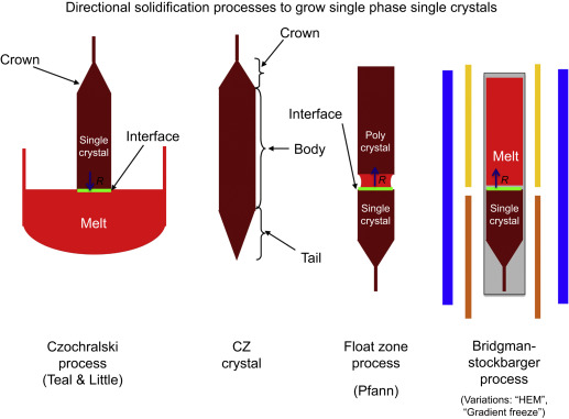
The hallmark of single crystal silicon is its uniform crystal lattice, achieved primarily through:
Key parameters like temperature control, pulling rate, and ambient atmosphere are tightly regulated to ensure defect-free crystal growth. Buyers should verify suppliers’ process control capabilities, as inconsistencies here directly affect wafer performance.
Once ingots are formed, they undergo:
The ability of a supplier to maintain tight tolerances during these steps is critical for downstream applications. Buyers should request detailed process parameters and wafer surface quality metrics.
For certain applications, wafers may be assembled into modules or packaged for integration. This stage includes:
Buyers interested in turnkey solutions should assess supplier expertise in assembly technologies and customization options.
Before shipment, wafers or assemblies undergo final finishing processes such as cleaning, drying, and protective coating application. This ensures longevity and handling safety.
Quality control in single crystal silicon manufacturing is governed by a combination of international standards and industry-specific certifications, which provide assurance of product consistency, safety, and performance.
B2B buyers should verify that suppliers hold certifications aligned with their industry and regional regulatory requirements.
Quality control is embedded throughout the manufacturing cycle, typically at three main checkpoints:
Buyers should confirm that suppliers employ automated inspection technologies and maintain detailed QC records for traceability.
To ensure single crystal silicon meets stringent performance criteria, suppliers employ a suite of testing methods:
Buyers should request sample test reports and inquire about the frequency and scope of testing protocols to ensure consistent quality.
For international buyers, especially from Africa, South America, the Middle East, and Europe (including markets like Mexico and Brazil), verifying supplier quality assurance involves a strategic approach:
When sourcing single crystal silicon across diverse regions, buyers should be mindful of several QC and compliance nuances:
By adopting these best practices, international B2B buyers can confidently source high-quality single crystal silicon tailored to their technological and market requirements.
Understanding the detailed cost structure and pricing dynamics of single crystal silicon is crucial for international B2B buyers aiming to optimize procurement strategies and negotiate favorable terms. This section breaks down the primary cost components, key price influencers, and practical buyer tips tailored to markets in Africa, South America, the Middle East, and Europe.
Illustrative Image (Source: Google Search)
Labor and Manufacturing Overhead
Labor costs vary widely by production location. Facilities with advanced automation may incur lower labor expenses but higher capital expenditure. Overhead includes utilities (notably electricity for crystal pulling processes), maintenance, and facility costs, which can fluctuate based on local energy prices and regulatory environments.
Tooling and Equipment Depreciation
Single crystal silicon production requires expensive, precision equipment such as Czochralski crystal pullers. The amortization of these capital investments is factored into unit costs, especially in smaller production runs or specialized customization.
Quality Control and Certifications
Rigorous QC processes—such as wafer inspection, electrical testing, and surface defect analysis—add to production costs. Achieving international certifications (e.g., ISO, RoHS compliance) can increase expenses but are often necessary for global market acceptance.
Logistics and Supply Chain Costs
Transporting fragile silicon wafers demands specialized packaging and handling, influencing cost. For buyers in Africa, South America, and the Middle East, logistics costs can be elevated due to longer shipping routes, customs duties, and port handling fees.
Illustrative Image (Source: Google Search)
Order Volume and Minimum Order Quantity (MOQ)
Bulk orders typically reduce per-unit costs through economies of scale. However, buyers from emerging markets should balance MOQ requirements against storage and capital constraints.
Technical Specifications and Customization
Custom wafer sizes, doping concentrations, or resistivity levels increase manufacturing complexity and costs. Standardized products are generally more cost-effective.
Material Grade and Purity
Higher purity and defect-free single crystal silicon wafers command premium pricing due to stricter processing requirements.
Quality Certifications and Compliance
Certifications required by specific industries (e.g., semiconductor, solar) add value and cost. Buyers should verify supplier credentials to avoid costly rejections.
Supplier Location and Reputation
Proximity can reduce lead times and freight costs. Trusted suppliers with proven delivery records often offer better long-term value despite higher upfront pricing.
Incoterms and Payment Terms
Terms such as FOB, CIF, or DDP impact who bears logistics risk and cost. Buyers must understand these to avoid unexpected expenses.
Negotiate Beyond Price
Focus on total value including lead times, payment flexibility, and after-sales support. In regions with volatile currency exchange (e.g., Brazil or South Africa), negotiating fixed-price contracts or multi-year agreements can mitigate financial risk.
Assess Total Cost of Ownership (TCO)
Incorporate logistics, customs duties, warehousing, and potential wastage into cost calculations. Often, the lowest unit price may not translate to the lowest TCO.
Leverage Group Buying and Local Partnerships
Buyers in Africa and South America can benefit from consortium purchasing or partnering with local distributors to reduce costs and improve supply chain resilience.
Understand Pricing Nuances in Your Region
Import tariffs, VAT, and local regulations vary significantly. For example, Middle Eastern buyers should consider free-trade zones and tax incentives that can impact landed costs.
Request Transparent Cost Breakdowns
Insist on detailed quotations breaking down raw material costs, overheads, and logistics to identify negotiation levers.
Plan for Quality Verification
Allocate budget and time for independent quality testing upon receipt to avoid downstream production losses.
Prices for single crystal silicon wafers are highly variable depending on specifications, order size, supplier, and geopolitical factors. The figures discussed here serve as indicative guidance only. Buyers should conduct due diligence and obtain multiple quotes tailored to their specific requirements.
By comprehensively analyzing these cost and pricing factors, international B2B buyers can make informed decisions, optimize procurement costs, and build resilient supply chains for single crystal silicon sourcing.
When sourcing single crystal silicon, understanding its core technical properties is essential for ensuring product quality, compatibility, and performance in your applications. Here are the key specifications that international B2B buyers should prioritize:
Material Grade
This defines the purity and crystalline quality of the silicon. Common grades include electronic-grade (ultra-high purity for semiconductors) and solar-grade (optimized for photovoltaic cells). Higher-grade silicon typically commands a premium but ensures better electrical properties and reliability. For buyers, selecting the correct grade aligns the material with end-use requirements, reducing defects and improving yield.
Resistivity
Measured in ohm-centimeters (Ω·cm), resistivity indicates how strongly the silicon opposes electric current. Low resistivity is crucial for semiconductor devices, while moderate resistivity suits photovoltaic applications. Understanding resistivity helps buyers specify materials that meet electrical performance targets and regulatory standards.
Crystal Orientation
Expressed in Miller indices (e.g., <100>, <111>), crystal orientation affects mechanical strength and electronic characteristics. For example, <100> orientation is preferred in integrated circuit manufacturing due to better etching properties. Buyers should confirm orientation specifications to ensure compatibility with manufacturing processes.
Wafer Thickness and Diameter
Typical wafer diameters range from 100 mm to 300 mm, with thickness varying according to application. Tolerance in thickness impacts device fabrication and mechanical handling. Accurate specifications prevent production delays and reduce scrap rates.
Dopant Concentration
Controlled doping with elements like boron or phosphorus tailors the electrical conductivity of silicon. The dopant type and concentration must be precisely specified, as they directly influence device functionality. Buyers should verify dopant levels to meet performance and compliance requirements.
Tolerance Levels
Tolerances define acceptable variations in dimensions and material properties. Tight tolerances ensure consistency and high yield, which are critical for large-scale manufacturing. Understanding tolerance specifications helps in negotiating quality standards and minimizing rejections.
Navigating the procurement process for single crystal silicon involves familiarity with key industry terms. These terms clarify expectations, streamline communication, and facilitate smooth transactions:
OEM (Original Equipment Manufacturer)
Refers to companies that produce parts or components used in another company’s final product. For silicon suppliers, knowing if you’re dealing with an OEM buyer helps tailor product specifications and volume commitments accordingly.
MOQ (Minimum Order Quantity)
The smallest quantity a supplier is willing to sell in one order. MOQs vary widely depending on production capabilities and material type. Understanding MOQ helps buyers plan inventory and negotiate better pricing or flexible order sizes.
RFQ (Request for Quotation)
A formal inquiry sent by buyers to suppliers to obtain pricing and terms for a specific quantity and specification of silicon. A clear, detailed RFQ accelerates supplier response times and ensures accurate quotes.
Incoterms (International Commercial Terms)
Standardized trade terms published by the International Chamber of Commerce that define responsibilities between buyers and sellers for shipping, insurance, and customs. Examples include FOB (Free On Board) and CIF (Cost, Insurance, and Freight). Familiarity with Incoterms reduces misunderstandings and clarifies cost and risk allocation.
Lead Time
The period between placing an order and receiving the product. Lead times for single crystal silicon can vary based on grade, quantity, and supplier capacity. Accurate lead time estimates are critical for production scheduling and supply chain management.
Traceability
The ability to track the silicon batch from raw material through processing to delivery. Traceability ensures quality control and compliance with industry standards, which is especially important for regulated sectors such as electronics and solar energy.
By mastering these technical properties and trade terms, B2B buyers across Africa, South America, the Middle East, and Europe can make informed procurement decisions, optimize costs, and build stronger supplier relationships. Clear specifications and terminology understanding reduce risks and enhance operational efficiency in sourcing single crystal silicon.
The single crystal silicon (SCS) market is a cornerstone of the global semiconductor and photovoltaic industries, driven by increasing demand for high-performance electronics and solar energy solutions. For international B2B buyers from regions such as Africa, South America, the Middle East, and Europe (including Mexico and Brazil), understanding the evolving market landscape is critical to securing competitive supply chains and leveraging growth opportunities.
Global Drivers: The surge in renewable energy adoption, particularly solar photovoltaic (PV) installations, is a primary growth engine for single crystal silicon. Governments across these regions are incentivizing clean energy projects, creating robust demand for high-purity silicon wafers used in solar cells. Additionally, the proliferation of consumer electronics, electric vehicles (EVs), and advanced semiconductors fuels the need for superior-quality SCS substrates.
Emerging Sourcing Trends: B2B buyers are increasingly prioritizing suppliers who offer integrated manufacturing capabilities, from silicon ingot growth to wafer slicing and polishing, ensuring consistent quality and traceability. There is a growing preference for just-in-time (JIT) delivery models to optimize inventory costs and reduce lead times. Moreover, digital platforms and blockchain technologies are being adopted to enhance transparency and streamline procurement processes.
Market Dynamics: Price volatility remains a key consideration due to fluctuations in raw material costs and geopolitical factors affecting silicon supply chains. Buyers from emerging markets should consider diversifying their supplier base to mitigate risks associated with trade restrictions and supply bottlenecks. Strategic partnerships with manufacturers in Asia and Europe can provide access to advanced technologies and foster innovation collaboration.
Sustainability is rapidly becoming a decisive factor in the sourcing of single crystal silicon, especially for B2B buyers aiming to meet environmental regulations and corporate social responsibility (CSR) goals. The production of single crystal silicon is energy-intensive, often involving high-temperature processes that contribute significantly to carbon emissions.
Illustrative Image (Source: Google Search)
Environmental Impact: Suppliers adopting renewable energy sources for silicon crystal growth and wafer processing can substantially reduce their carbon footprint. Additionally, innovations in recycling silicon kerf (waste silicon particles from wafer slicing) are gaining traction, allowing for the recovery and reuse of valuable materials.
Ethical Supply Chains: Transparency in the supply chain is paramount. Buyers should seek suppliers who comply with internationally recognized standards such as ISO 14001 (environmental management) and ISO 45001 (occupational health and safety). Ensuring fair labor practices and avoiding conflict minerals in raw material sourcing is also critical to maintaining ethical standards.
Green Certifications and Materials: Certifications like the Responsible Minerals Initiative (RMI) and adherence to the International Electrotechnical Commission (IEC) standards for photovoltaic materials provide assurance of sustainability. Some suppliers now offer “green silicon” produced with minimal environmental impact, appealing to buyers committed to sustainable procurement.
Single crystal silicon technology has evolved significantly since its inception in the mid-20th century. Initially developed for semiconductor applications, the Czochralski process became the standard for producing high-purity silicon ingots. Over decades, advancements in crystal growth and wafer slicing technologies have dramatically improved material quality and yield.
For B2B buyers, understanding this evolution highlights the importance of selecting suppliers with cutting-edge manufacturing capabilities. The transition from multi-crystalline to single crystal silicon in solar PV has also underscored the material’s superior efficiency, driving widespread adoption in global renewable energy markets.
This historical perspective underscores how technological progress, combined with shifting market demands, continues to shape sourcing strategies and supply chain resilience in the single crystal silicon sector.
How can I effectively vet suppliers of single crystal silicon for international procurement?
When sourcing single crystal silicon internationally, particularly from diverse regions such as Africa, South America, the Middle East, and Europe, thorough supplier vetting is crucial. Start by verifying certifications like ISO 9001 and industry-specific quality standards. Request detailed technical datasheets and sample batches to assess product consistency. Check the supplier’s track record with international clients and their capacity to meet your volume and customization needs. Engaging with trade references and conducting factory audits—either in-person or via trusted third parties—can significantly reduce risk and ensure reliability in long-term partnerships.
What customization options are available for single crystal silicon, and how can I communicate my specific requirements?
Single crystal silicon can be customized in wafer size, thickness, doping type, resistivity, and surface finish to suit various industrial applications. Clearly articulate your technical specifications, including crystallographic orientation and impurity levels, in your initial RFQ. Providing detailed drawings or reference standards helps avoid misunderstandings. Collaborate closely with suppliers experienced in customization, as they can advise on feasibility and potential impacts on cost and lead time. Establishing clear communication channels early ensures your product meets precise application needs and regulatory requirements.
What are typical minimum order quantities (MOQ), lead times, and payment terms for international single crystal silicon orders?
MOQ for single crystal silicon varies by supplier and product type but generally ranges from small batch orders of a few hundred wafers to several thousand for standard sizes. Lead times typically span 4 to 12 weeks, influenced by customization and production capacity. Payment terms often include a 30-50% upfront deposit with the balance due upon shipment or delivery. Negotiation is common, especially for repeat orders or larger volumes. Buyers should factor in lead times for customs clearance and shipping when planning procurement schedules to maintain supply chain continuity.
Which quality assurance certifications and testing protocols should I expect from reputable single crystal silicon suppliers?
Top-tier suppliers provide quality assurance backed by ISO 9001 certification and compliance with semiconductor industry standards such as SEMI or IEC. Expect comprehensive testing reports covering crystallographic quality, electrical properties, surface defects, and contamination levels. Third-party inspection certificates or factory QA audits add transparency. For critical applications, consider suppliers offering batch traceability and failure analysis support. Insisting on documented quality control processes reduces the risk of receiving substandard materials that could compromise your manufacturing output.
What logistics considerations are critical when importing single crystal silicon from regions like Africa or South America?
Logistics for single crystal silicon demand careful handling due to its fragile nature and sensitivity to contamination. Use specialized packaging designed to prevent mechanical damage and electrostatic discharge. Choose reliable freight forwarders experienced in handling high-value, delicate semiconductor materials. Be aware of local customs regulations, import duties, and potential delays at ports, which vary across regions such as Africa and South America. Incorporate buffer times in your supply chain planning and consider incoterms that allocate risk and responsibility clearly between buyer and seller.
How should disputes related to product quality or delivery issues be managed in international single crystal silicon transactions?
Establish clear contract terms specifying quality criteria, delivery schedules, and dispute resolution mechanisms before finalizing orders. In case of disputes, document all communications and discrepancies thoroughly, including photographic evidence and test results. Engage suppliers promptly to negotiate solutions such as replacement shipments or refunds. Utilizing international arbitration bodies or trade chambers in your region can facilitate impartial resolution. Building trust through transparent communication and fair handling of disputes strengthens long-term supplier relationships and minimizes operational disruptions.
What payment methods are safest and most effective for international B2B purchases of single crystal silicon?
Letters of credit (LCs) and escrow services offer robust protection for both buyers and suppliers by ensuring payment is made only upon fulfillment of agreed conditions. Wire transfers are common but carry higher risk if contractual safeguards are weak. For new suppliers, consider staged payments tied to production milestones. Digital payment platforms with buyer protection policies can also be useful but verify their acceptance in your supplier’s country. Always align payment methods with your risk tolerance and legal advice to safeguard your investment in high-value materials.
How can buyers in emerging markets optimize costs when sourcing single crystal silicon internationally?
Cost optimization begins with consolidating orders to meet supplier MOQs and negotiating volume discounts. Engage multiple suppliers across regions like Europe and Asia to compare pricing and lead times. Consider total landed cost, including tariffs, shipping, and local taxes, rather than focusing solely on unit price. Leveraging local trade agreements or free trade zones can reduce import duties. Collaborate with logistics partners to optimize shipping routes and reduce delays. Lastly, investing in long-term supplier relationships often results in better pricing, priority production slots, and improved after-sales support.
The information provided in this guide, including content regarding manufacturers, technical specifications, and market analysis, is for informational and educational purposes only. It does not constitute professional procurement advice, financial advice, or legal advice.
While we have made every effort to ensure the accuracy and timeliness of the information, we are not responsible for any errors, omissions, or outdated information. Market conditions, company details, and technical standards are subject to change.
B2B buyers must conduct their own independent and thorough due diligence before making any purchasing decisions. This includes contacting suppliers directly, verifying certifications, requesting samples, and seeking professional consultation. The risk of relying on any information in this guide is borne solely by the reader.
Strategic sourcing of single crystal silicon is pivotal for international B2B buyers aiming to secure high-quality, cost-effective materials that meet stringent industry standards. Key takeaways highlight the importance of evaluating supplier reliability, understanding regional supply chain dynamics, and leveraging technological advancements to optimize procurement. For buyers in Africa, South America, the Middle East, and Europe, including markets like Mexico and Brazil, cultivating strong supplier relationships and diversifying sourcing channels can mitigate risks associated with market volatility and geopolitical shifts.
Emphasizing strategic partnerships and transparent communication enables buyers to anticipate supply disruptions and align product specifications with evolving industry demands. Additionally, staying informed about sustainability trends and regulatory changes will enhance compliance and corporate responsibility, increasingly valued in global trade.
Looking ahead, the single crystal silicon market is poised for innovation-driven growth, with emerging applications in renewable energy and electronics expanding demand. International buyers are encouraged to adopt a proactive sourcing strategy that integrates market intelligence, supplier collaboration, and risk management. By doing so, they can not only secure supply continuity but also position their businesses competitively in an evolving global landscape. Engage with trusted partners today to harness the full potential of single crystal silicon for your enterprise’s future success.
Tags: Black Silicon Carbide, White Fused Alumina, Brown Fused Alumina, Pink Fused Alumina, Black Fused Alumina