Navigating the complexities of sourcing density silicon can be a significant challenge for international B2B buyers, particularly those operating in emerging markets across Africa, South America, the Middle East, and Europe. With a density of approximately 2.329 g/cm³, silicon is not just a fundamental element in semiconductor manufacturing; it also serves a myriad of applications in electronics, renewable energy, and advanced materials. This guide provides a comprehensive overview of density silicon, covering essential topics such as types of silicon products, their applications, supplier vetting processes, and cost considerations.
By equipping B2B buyers with in-depth knowledge about silicon’s properties and market dynamics, this guide empowers them to make informed purchasing decisions. Whether you are a buyer in Colombia seeking reliable suppliers or a business in South Africa looking to optimize your silicon procurement strategy, understanding the nuances of density silicon will enhance your competitive edge. Furthermore, we address regional market trends, regulatory considerations, and quality assurance practices that are crucial for successful international transactions.
As you delve deeper into this guide, you will discover actionable insights that help streamline your sourcing processes and mitigate risks, ultimately contributing to your business's growth and innovation in the global market.
| Type Name | Key Distinguishing Features | Primary B2B Applications | Brief Pros & Cons for Buyers |
|---|---|---|---|
| Crystalline Silicon | High density (2.329 g/cm³), diamond cubic structure | Semiconductor devices, solar cells | Pros: High performance, excellent thermal conductivity. Cons: Higher cost due to purity requirements. |
| Amorphous Silicon | Non-crystalline, lower density, flexible | Thin-film solar panels, flexible electronics | Pros: Versatile, cost-effective for large areas. Cons: Lower efficiency compared to crystalline types. |
| Polycrystalline Silicon | Composed of multiple small crystals, moderate density | Solar panels, electronic components | Pros: Cost-effective, good balance of efficiency and price. Cons: Slightly lower efficiency than single-crystal. |
| Doped Silicon | Silicon with impurities to enhance conductivity | High-performance electronics, sensors | Pros: Tailored electrical properties, crucial for device performance. Cons: May affect mechanical integrity. |
| Silicon Carbide | Higher density (3.21 g/cm³), extreme hardness | High-temperature applications, power devices | Pros: Excellent thermal and chemical stability. Cons: More expensive and challenging to process. |
Crystalline silicon is the most common type used in semiconductor manufacturing, characterized by its high density of 2.329 g/cm³ and a diamond cubic crystal structure. This structure provides exceptional thermal conductivity and mechanical strength, making it ideal for high-performance applications such as semiconductor devices and solar cells. Buyers should consider the high purity requirements and associated costs, which can impact overall project budgets.
Amorphous silicon lacks a defined crystalline structure, resulting in a lower density and flexibility. This type is primarily used in thin-film solar panels and flexible electronics due to its ability to cover large areas efficiently. While it is more cost-effective than crystalline silicon, its lower energy conversion efficiency is a crucial consideration for buyers focused on performance.
Polycrystalline silicon consists of numerous small silicon crystals, offering a balance between cost and efficiency. With a moderate density, it is widely utilized in solar panels and various electronic components. Buyers appreciate its lower manufacturing costs compared to single-crystal silicon, although it may yield slightly lower efficiency rates. Understanding the trade-offs between cost and performance is essential for informed purchasing decisions.
Doped silicon incorporates impurities to enhance its electrical properties, making it vital in the production of high-performance electronic devices and sensors. This type allows for customized conductivity levels, which is crucial for various applications. However, buyers should be aware that doping can sometimes compromise the mechanical integrity of silicon, requiring careful consideration of the application requirements.
Silicon carbide (SiC) is a high-density material (3.21 g/cm³) known for its extreme hardness and thermal stability. Its unique properties make it suitable for high-temperature and high-power applications, such as power devices and automotive components. While SiC offers significant advantages in performance, its higher processing costs and complexity may deter some buyers. Understanding the specific application needs and budget constraints is key to making an informed decision.
| Industry/Sector | Specific Application of Density Silicon | Value/Benefit for the Business | Key Sourcing Considerations for this Application |
|---|---|---|---|
| Semiconductor Manufacturing | Silicon Wafers for Integrated Circuits | High performance in electronics, enabling faster devices | Quality control, purity levels, and precise dimensions |
| Solar Energy | Photovoltaic Cells | Efficient energy conversion, reducing operational costs | Supplier reliability, material sourcing, and certifications |
| Aerospace and Defense | Structural Components in Satellites | Enhanced durability and lightweight solutions | Compliance with international standards and testing |
| Automotive Industry | Electric Vehicle Components | Improved efficiency and reduced weight | Long-term supply agreements and scalability |
| Consumer Electronics | High-Performance Transistors | Increased device reliability and performance | Cost-effectiveness and technological advancements |
In semiconductor manufacturing, density silicon is primarily utilized in the production of silicon wafers, which serve as the substrate for integrated circuits. The high density of silicon contributes to its strength and thermal conductivity, essential for effective heat dissipation in electronic devices. For international buyers, especially in regions like Africa and South America, sourcing high-purity silicon wafers is crucial. They must ensure that suppliers maintain strict quality control measures to avoid defects that can lead to significant production losses.
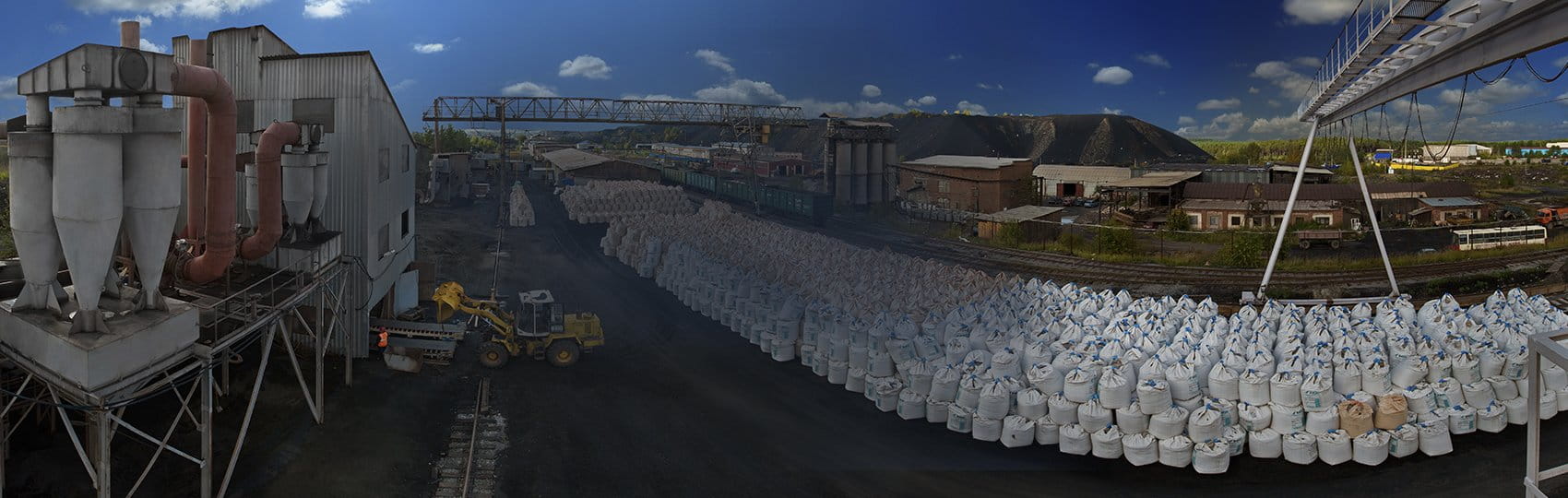
A stock image related to density silicon.
Density silicon is a critical component in photovoltaic cells used in solar panels. Its high density and intrinsic properties enable efficient light absorption and energy conversion, making solar energy a viable alternative to fossil fuels. For buyers in the Middle East and Europe, the focus should be on sourcing solar-grade silicon that meets international standards. This includes verifying supplier certifications and assessing the environmental impact of the production processes to ensure sustainability.
In the aerospace and defense sectors, density silicon is employed in structural components for satellites and other high-performance applications. The material's exceptional strength-to-weight ratio and thermal stability make it ideal for use in extreme conditions. International B2B buyers need to consider compliance with stringent aerospace standards and require detailed documentation of material properties and testing results to ensure safety and reliability.
A stock image related to density silicon.
Density silicon is increasingly being used in electric vehicle (EV) components, including power electronics and battery management systems. Its properties allow for lighter and more efficient designs, contributing to improved vehicle performance and range. Buyers from Europe and South America should prioritize suppliers that can offer scalable solutions and long-term partnerships, as the demand for EV components continues to rise.
In consumer electronics, high-performance transistors made from density silicon are essential for the reliability and efficiency of devices such as smartphones and laptops. The material's high density supports faster processing speeds and better thermal management. For international buyers, particularly in emerging markets, sourcing innovative silicon technologies at competitive prices is vital. They should also evaluate the technological advancements of suppliers to ensure they remain competitive in the fast-evolving electronics market.
Related Video: The Ultimate Guide to Silicon Dioxide: Specifications, Uses, and Benefits. Industrial Chemistry.
The Problem:
B2B buyers in the semiconductor industry often encounter challenges related to the variability of silicon density when sourcing materials for wafer fabrication. Variations can stem from factors such as temperature changes during production, impurities in the silicon, or the specific fabrication processes employed. These inconsistencies can lead to defects in the final products, impacting yield and performance, which is especially critical for high-stakes applications in electronics and telecommunications.
The Solution:
To mitigate issues arising from density variability, buyers should prioritize sourcing silicon from reputable suppliers who employ stringent quality control measures. It’s advisable to request detailed documentation on the silicon’s density measurements and production processes. Moreover, engaging suppliers that utilize advanced techniques like isotopic purification can help ensure more consistent density levels. Buyers should also consider investing in internal capabilities to monitor and measure density during their own fabrication processes, allowing for real-time adjustments and quality assurance.
The Problem:
When utilizing doped silicon for specific applications, such as creating p-type or n-type semiconductors, buyers often face challenges due to the effects of doping on silicon density. The presence of dopants can lead to slight changes in density, which may not be immediately apparent but can significantly affect the electrical properties and overall performance of semiconductor devices. This situation complicates the design and manufacturing processes, especially when precise specifications are required.
The Solution:
To address the impact of doping on silicon density, it is crucial for buyers to collaborate closely with their suppliers to understand the specific characteristics of the doped silicon they are procuring. Buyers should specify the exact doping levels and types to ensure compatibility with their processes. Implementing thorough testing and characterization protocols can help quantify how the doping affects density and performance. Buyers can also explore alternative materials or different doping techniques that could yield a more stable density profile, thus enhancing the performance of their semiconductor applications.
The Problem:
B2B buyers involved in silicon wafer production frequently encounter issues related to temperature fluctuations during the manufacturing process. These fluctuations can alter the density of silicon, leading to inconsistencies in wafer quality and performance. Such variability can result in increased waste, higher production costs, and delays in delivery timelines, which are detrimental in fast-paced markets like consumer electronics.
The Solution:
To combat the challenges posed by temperature variations, buyers should invest in robust temperature control systems throughout their manufacturing facilities. Implementing real-time monitoring and automated adjustments can significantly stabilize the production environment. Additionally, selecting suppliers who utilize advanced thermal management techniques during the crystal growth and wafer slicing processes can ensure that the silicon maintains its intrinsic density. Buyers should also consider developing a comprehensive training program for their teams on the importance of temperature management and its direct impact on silicon density, fostering a culture of quality and precision in production.
When selecting materials for applications involving density silicon, international B2B buyers must consider various factors that influence performance, cost, and compliance. Below is an analysis of four common materials used in conjunction with density silicon, focusing on their key properties, advantages, disadvantages, and specific considerations for buyers from Africa, South America, the Middle East, and Europe.
Silicon (Si)
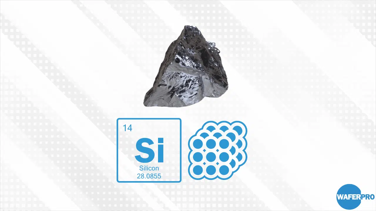
Silicon is a fundamental material in the semiconductor industry, known for its high density of 2.329 g/cm³. Its properties include excellent thermal conductivity, high melting point (1415°C), and good mechanical strength. Silicon's crystalline structure allows for efficient packing and high rigidity, making it suitable for various electronic applications.
Silicon Carbide (SiC)
Silicon carbide is a compound semiconductor that exhibits superior thermal conductivity and a higher breakdown electric field than silicon. It is often used in high-temperature and high-voltage applications.
Gallium Arsenide (GaAs)
Gallium arsenide is another semiconductor material with a density of approximately 5.32 g/cm³. It is known for its high electron mobility and efficiency in converting electricity to light, making it ideal for optoelectronic devices.
Germanium (Ge)
Germanium is a less common semiconductor material with a density of 5.32 g/cm³. It is primarily used in high-speed electronics and fiber optics due to its high carrier mobility.
International B2B buyers, particularly from regions like Africa, South America, the Middle East, and Europe, should pay attention to compliance with common standards such as ASTM, DIN, and JIS. Additionally, understanding local regulations regarding material sourcing, environmental impact, and safety is crucial. Buyers should also consider the availability of materials and the associated costs, as these can vary significantly by region.
| Material | Typical Use Case for density silicon | Key Advantage | Key Disadvantage/Limitation | Relative Cost (Low/Med/High) |
|---|---|---|---|---|
| Silicon (Si) | Microchips, solar cells | High thermal conductivity | Brittle nature can lead to breakage | Low |
| Silicon Carbide (SiC) | High-voltage electronics | Exceptional thermal stability | Higher manufacturing costs | High |
| Gallium Arsenide (GaAs) | Optoelectronic devices | High efficiency in light emission | Toxicity of arsenic raises concerns | High |
| Germanium (Ge) | High-speed electronics, fiber optics | Excellent electronic properties | Less abundant and more expensive | Medium |
This guide provides a comprehensive overview of key materials associated with density silicon, helping international B2B buyers make informed decisions based on performance, cost, and compliance considerations.
The manufacturing of density silicon involves several critical stages, each designed to ensure the optimal properties of the final product. These stages include material preparation, forming, assembly, and finishing.
Material Preparation:
In this initial phase, high-purity silicon feedstock is sourced. The most common feedstock is metallurgical-grade silicon, which undergoes purification through processes such as the Siemens process or the Czochralski method. Impurities are minimized to achieve the desired density and electrical characteristics. The silicon is then melted in a controlled environment to maintain purity.
Forming:
Once prepared, the molten silicon is shaped into ingots or wafers using techniques such as the Czochralski method or float-zone processing. The Czochralski method involves pulling a seed crystal from the molten silicon to form a single crystal ingot, while float-zone processing allows for the production of high-purity single crystals without the introduction of contaminants. This stage is crucial for achieving the high density of silicon, typically around 2.329 g/cm³.
Assembly:
After forming, the silicon wafers are sliced into thin disks. Precision is essential here, as any inconsistency can affect the performance of semiconductor devices. Advanced diamond wire saws are often used to minimize kerf loss and enhance yield. This stage may also involve doping processes, where specific impurities are introduced to modify electrical properties.
Finishing:
The final stage involves lapping, polishing, and cleaning the silicon wafers to achieve the desired surface finish. This process is vital for ensuring high-quality performance in electronic applications. Proper mechanical polishing techniques are applied to maintain uniform thickness and surface integrity, which are critical for subsequent fabrication processes.
Quality control (QC) is paramount in the manufacturing process of density silicon. It ensures that the final product meets international standards and customer specifications.
International Standards Compliance:
Adherence to standards such as ISO 9001 is essential for manufacturers. This standard focuses on quality management systems and continuous improvement. In addition, industry-specific standards like CE marking for products sold in Europe or API specifications for certain applications are also crucial. These certifications assure buyers of the product's quality and compliance with safety regulations.
Quality Control Checkpoints:
The QC process typically includes several checkpoints:
- Incoming Quality Control (IQC): This involves inspecting raw materials and components before they enter the production process. Ensuring that the silicon feedstock meets purity and density specifications is critical.
- In-Process Quality Control (IPQC): During manufacturing, regular checks are conducted to monitor critical parameters such as temperature, density, and impurity levels. This ensures that the manufacturing process remains within acceptable limits.
- Final Quality Control (FQC): After the wafers are produced, they undergo comprehensive testing for physical and electrical properties. This may include density measurements, resistivity tests, and surface inspections.
Common Testing Methods for Silicon Quality Assurance:
Various testing methods are employed to ensure product quality:
- Density Measurement: Techniques such as Archimedes' principle or hydrostatic weighing are used to accurately determine the density of silicon wafers.
- Electrical Testing: The wafers are tested for carrier concentration and mobility, which are vital for semiconductor performance.
- Surface Roughness Testing: Atomic force microscopy (AFM) or optical profilers may be used to assess surface quality, which impacts device performance.
For international B2B buyers, particularly from regions like Africa, South America, the Middle East, and Europe, ensuring supplier quality is critical for maintaining production standards.
Conducting Audits:
Regular supplier audits are an effective way to assess compliance with quality standards. Buyers should request documentation of quality management systems and previous audit reports. This practice helps in identifying potential risks and ensuring that suppliers adhere to required standards.
Reviewing Quality Reports:
Suppliers should provide detailed quality reports, including data from IQC, IPQC, and FQC processes. These reports should clearly outline the results of various tests, including density measurements and defect rates. Analyzing these reports allows buyers to gauge the reliability and consistency of the supplier's output.
Utilizing Third-Party Inspections:
Engaging third-party inspection services can provide an unbiased assessment of the supplier's quality control processes. These inspections can cover everything from raw material sourcing to finished product testing, ensuring that all aspects of the manufacturing process meet international standards.
When dealing with international suppliers, B2B buyers must be aware of several nuances regarding quality control:
Cultural Differences in Quality Standards:
Understanding that different regions may have varying perceptions of quality can help buyers set realistic expectations. For example, European suppliers may adhere to stricter environmental regulations than those in other regions.
Regulatory Compliance:
Buyers should ensure that suppliers are compliant with local regulations and international standards, particularly when sourcing from countries with less stringent oversight. This includes understanding any unique requirements that may apply in specific markets, such as the Middle East or South America.
Communication and Transparency:
Establishing clear communication channels with suppliers is vital. Buyers should encourage transparency regarding production methods and quality assurance processes. Regular updates and open lines of communication can significantly enhance trust and collaboration.
Understanding the intricacies of the manufacturing processes and quality assurance for density silicon is essential for international B2B buyers. By focusing on key manufacturing stages, adhering to rigorous quality control measures, and verifying supplier practices, buyers can ensure they source high-quality silicon that meets their specific needs. This diligence not only enhances product reliability but also strengthens partnerships across diverse markets, from Africa to Europe and beyond.
This guide provides a practical checklist for international B2B buyers focused on procuring density silicon. Understanding the key steps in sourcing this essential material can streamline your procurement process and ensure that you partner with reliable suppliers who meet your specific needs.
Clearly outline your requirements for density silicon. This includes specifying the desired density (typically around 2.329 g/cm³), purity levels, and any specific applications (e.g., semiconductor manufacturing). Knowing your exact needs helps in identifying suitable suppliers and ensures that the silicon you procure meets industry standards.
Conduct thorough research to identify potential suppliers. Utilize industry directories, trade shows, and online platforms to compile a list of manufacturers and distributors specializing in silicon. Look for suppliers with a solid reputation in the market, particularly those that cater to buyers in your region, such as Africa, South America, the Middle East, and Europe.
Ensure that your selected suppliers have the necessary certifications. Certifications such as ISO 9001 for quality management systems and ISO 14001 for environmental management demonstrate a supplier's commitment to quality and sustainability. This step is crucial as it mitigates risks associated with quality control and compliance with international standards.
Assess the production capabilities of your shortlisted suppliers. Review their manufacturing processes, technology used, and capacity to deliver large orders. It's also beneficial to understand their quality assurance procedures, as this will impact the consistency and quality of the silicon supplied.
Obtain samples for testing before making a bulk purchase. This allows you to evaluate the physical and chemical properties of the silicon, ensuring it meets your specifications. Consider conducting density measurements and other relevant tests to confirm that the silicon performs well in your intended applications.
Discuss pricing structures and payment terms with potential suppliers. Be sure to compare quotes from multiple suppliers while considering the overall value, including shipping costs, delivery timelines, and payment flexibility. Transparent pricing and favorable terms can significantly impact your procurement budget and cash flow management.
Ensure clear communication channels with your chosen supplier. Establishing effective lines of communication can facilitate quick resolution of issues that may arise during the procurement process. Additionally, inquire about after-sales support and technical assistance, which can be invaluable for troubleshooting and optimizing the use of the silicon in your operations.
By following this checklist, B2B buyers can navigate the complexities of sourcing density silicon effectively, ultimately leading to successful procurement outcomes.
When sourcing density silicon, international B2B buyers should consider various cost components that contribute to the overall pricing structure. These include:
Materials: The primary cost driver is the raw material itself. Silicon prices can fluctuate based on market demand, purity levels, and sourcing regions. High-purity silicon, essential for semiconductor applications, can command a premium.
Labor: Labor costs vary significantly across regions. For instance, labor costs in South America may differ from those in Europe or Africa, influencing the overall pricing model.
Manufacturing Overhead: This encompasses indirect costs associated with production, including utilities, facility maintenance, and administrative expenses. Efficient manufacturing processes can help reduce these overhead costs.
Tooling: The initial investment in specialized tools and machinery for silicon processing can be substantial. Buyers should assess whether suppliers utilize the latest technologies that can enhance production efficiency and lower long-term costs.
Quality Control (QC): Rigorous QC processes ensure that the silicon meets required specifications, adding to the overall cost. Buyers should inquire about the QC measures implemented by suppliers to guarantee product reliability.
Logistics: Transportation and shipping costs can significantly impact the total cost, especially for international buyers. Factors such as distance, mode of transport, and import duties must be considered.
Margin: Supplier margins will vary based on market conditions and competition. Understanding the supplier's pricing strategy can aid in negotiations.
Several factors influence the price of density silicon, which B2B buyers must carefully evaluate:
Volume and Minimum Order Quantity (MOQ): Higher purchase volumes typically result in lower unit costs due to economies of scale. Buyers should negotiate MOQs that align with their production needs.
Specifications and Customization: Custom silicon products tailored to specific applications may incur additional costs. Buyers must weigh the benefits of customization against potential price increases.
Material Quality and Certifications: Higher-quality silicon, often with certifications for purity and performance, can come at a premium. Buyers should assess whether the added cost aligns with their application requirements.
Supplier Factors: The reputation, reliability, and geographical location of suppliers can impact pricing. Established suppliers may charge higher prices due to their proven track record and quality assurance.
Incoterms: Understanding Incoterms is crucial for international transactions. They define the responsibilities of buyers and sellers concerning shipping, insurance, and tariffs, which can affect overall costs.
International B2B buyers, particularly in Africa, South America, the Middle East, and Europe, can adopt several strategies to enhance cost efficiency when sourcing density silicon:
Effective Negotiation: Engage suppliers in discussions about pricing, especially when placing large orders. Leverage competitive quotes to negotiate better terms.
Assess Total Cost of Ownership (TCO): Beyond the initial purchase price, consider long-term costs associated with quality, reliability, and maintenance. A lower upfront cost may lead to higher TCO if the product does not meet performance expectations.
Understand Pricing Nuances for International Transactions: Currency fluctuations and geopolitical factors can impact pricing. Buyers should stay informed about market trends and adjust their purchasing strategies accordingly.
Build Strong Supplier Relationships: Establishing long-term partnerships can lead to better pricing and terms. Suppliers may offer discounts or favorable conditions to loyal customers.
While sourcing density silicon, international buyers must navigate a complex landscape of cost components and price influencers. By understanding these factors and employing effective negotiation strategies, they can optimize their sourcing decisions, ensuring they achieve the best value for their investments. Keep in mind that prices can vary widely based on specifications and market conditions, so thorough market research and supplier evaluation are essential.
In the rapidly evolving landscape of materials for semiconductor manufacturing, understanding the alternatives to density silicon is crucial for B2B buyers. While density silicon boasts numerous advantages, several alternative materials and methods can also meet various application requirements. This section will compare density silicon against two viable alternatives: Germanium and Gallium Arsenide.
| Comparison Aspect | Density Silicon | Germanium | Gallium Arsenide |
|---|---|---|---|
| Performance | High thermal conductivity, excellent electron mobility | Good thermal properties, lower electron mobility than silicon | Excellent electron mobility, high efficiency in optoelectronic applications |
| Cost | Moderate; widely produced | Higher cost due to limited supply and production | High cost; specialized manufacturing processes |
| Ease of Implementation | Well-established processes | More complex due to brittleness | Requires specialized techniques for growth and fabrication |
| Maintenance | Low; stable under normal conditions | Moderate; sensitivity to oxidation | Moderate; requires careful handling to prevent degradation |
| Best Use Case | General semiconductor applications, integrated circuits | High-speed electronics, infrared optics | High-efficiency solar cells, optoelectronics |
Germanium is another semiconductor material with unique properties that can sometimes outperform silicon. Its high intrinsic carrier mobility makes it suitable for high-speed electronics and applications requiring infrared optics. However, the cost of germanium is typically higher than that of density silicon, primarily due to its limited availability and complex production processes. Additionally, germanium's brittleness can pose challenges during manufacturing and implementation, making it less favorable for some applications.
Gallium Arsenide (GaAs) is known for its exceptional electron mobility and efficiency in optoelectronic applications, such as LEDs and solar cells. Its performance in high-frequency applications is superior to that of density silicon. However, GaAs comes at a higher price point, and its manufacturing processes are more specialized, which can lead to increased costs for B2B buyers. Furthermore, GaAs materials require careful handling to prevent degradation, which can add to maintenance efforts over time.
When evaluating density silicon against alternatives like germanium and gallium arsenide, B2B buyers should consider their specific application requirements. For general semiconductor applications, density silicon remains a strong choice due to its balance of cost, performance, and established manufacturing processes. However, for specialized applications such as high-speed electronics or optoelectronics, investing in germanium or gallium arsenide may yield superior results despite higher costs. Ultimately, understanding the unique properties and trade-offs of each material will empower buyers to make informed decisions that align with their operational goals and budget constraints.
When dealing with density silicon, understanding its essential technical properties is crucial for making informed purchasing decisions. Here are some critical specifications:
Density (kg/m³)
The density of silicon is approximately 2,329 kg/m³. This property is vital as it influences the material's weight, which can affect shipping costs and storage requirements. For B2B buyers, knowing the density helps in calculating the volume needed for production processes and ensures compliance with product specifications.
Purity Grade
Silicon is available in various purity grades, often expressed as a percentage. High-purity silicon (≥99.9999%) is essential for semiconductor applications, while lower grades may suffice for other uses. Buyers must specify the required purity level to ensure compatibility with their manufacturing processes and to avoid costly defects.
Thermal Conductivity (W/m·K)
Silicon's thermal conductivity is around 150 W/m·K at room temperature. This property is critical for applications in electronics where heat dissipation is crucial. Understanding thermal conductivity helps buyers select the appropriate silicon for high-performance applications, ensuring device reliability and longevity.
Mechanical Properties (Tensile Strength)
The tensile strength of silicon is approximately 7 GPa. This property indicates how much stress silicon can withstand before breaking, which is essential for applications requiring durability. Buyers should consider the mechanical properties to match the silicon's strength with their application needs, especially in structural components.
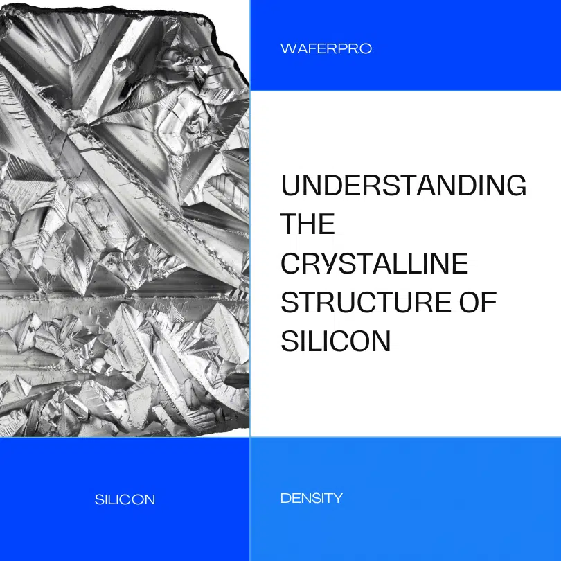
Crystal Structure
Silicon crystallizes in a diamond cubic structure, which contributes to its high density and mechanical strength. This structural property is vital in semiconductor manufacturing, where crystal quality can significantly impact device performance. B2B buyers should prioritize suppliers who can guarantee high-quality crystalline silicon to enhance product efficiency.
Understanding industry jargon is equally important for B2B buyers in navigating the procurement process. Here are some common terms:
OEM (Original Equipment Manufacturer)
OEM refers to companies that produce components that are used in another company's end product. Understanding this term is crucial for buyers who may be sourcing silicon for integration into larger systems, as it often affects quality standards and specifications.
MOQ (Minimum Order Quantity)
MOQ is the smallest quantity of a product that a supplier is willing to sell. Knowing the MOQ is essential for buyers to manage inventory effectively and to assess whether a supplier fits their purchasing strategy.
RFQ (Request for Quotation)
An RFQ is a document sent to suppliers requesting a quote for specific quantities of silicon at defined specifications. This term is vital for buyers to understand as it initiates the procurement process and ensures accurate pricing and delivery terms.
Incoterms
Incoterms are international commercial terms that define the responsibilities of buyers and sellers in shipping goods. Familiarity with Incoterms helps buyers understand shipping costs, risk management, and delivery responsibilities, which are critical for international transactions, especially when dealing with suppliers from diverse regions like Africa, South America, the Middle East, and Europe.
Lead Time
Lead time refers to the amount of time it takes from placing an order to receiving the product. For B2B buyers, understanding lead times is crucial for planning production schedules and maintaining inventory levels, especially in industries where timing is critical.
By grasping these technical properties and trade terminologies, international B2B buyers can make more informed decisions when sourcing density silicon, ensuring compatibility with their applications and optimizing their supply chain operations.
The density silicon market is currently experiencing significant growth driven by the increasing demand for semiconductor devices, particularly in emerging markets in Africa, South America, the Middle East, and Europe. Key drivers include the proliferation of electronic devices and the shift towards renewable energy technologies, which require high-quality silicon for photovoltaic cells. As international B2B buyers, particularly from regions like Colombia and Brazil, navigate this landscape, understanding the dynamics of silicon sourcing becomes crucial.
Emerging trends include a shift towards vertically integrated supply chains, allowing manufacturers to control the quality and consistency of silicon. Additionally, advancements in wafer fabrication technology are leading to increased efficiency and reduced waste, making it essential for buyers to consider suppliers that invest in these technologies. Furthermore, the growing emphasis on customization in silicon products is prompting suppliers to offer tailored solutions that meet specific industry needs, from consumer electronics to automotive applications.
Buyers should also be aware of geopolitical factors impacting silicon supply chains. Trade policies, tariffs, and regional regulations can affect sourcing strategies, making it vital to stay informed about the political landscape. By leveraging data analytics and market intelligence, B2B buyers can make informed decisions and secure advantageous procurement agreements.
Sustainability and ethical sourcing are becoming increasingly important for B2B buyers in the density silicon sector. As environmental concerns rise globally, companies are under pressure to demonstrate their commitment to sustainable practices. The extraction and processing of silicon can have significant environmental impacts, including habitat destruction and carbon emissions. Therefore, buyers must prioritize suppliers who adhere to sustainable practices, such as responsible mining and energy-efficient manufacturing processes.
Certifications and standards play a vital role in ensuring ethical sourcing. Look for suppliers that hold certifications like ISO 14001 (Environmental Management) or those involved in initiatives promoting responsible sourcing. Additionally, some manufacturers are now offering 'green' silicon products that utilize recycled materials or renewable energy in their production processes. By choosing these options, B2B buyers can not only reduce their carbon footprint but also enhance their brand reputation.
Moreover, engaging with suppliers who value transparency in their supply chains can lead to more resilient partnerships. Buyers should conduct due diligence to ensure that their sourcing practices align with corporate social responsibility (CSR) goals, which can improve overall business performance and customer loyalty.
The evolution of the density silicon sector has been marked by technological advancements and shifts in market demand. Initially, silicon was primarily used in the manufacturing of basic electronic components. However, with the advent of the digital age, the demand for high-purity silicon for semiconductor applications surged. This led to innovations in crystal growth methods, such as the Czochralski process, which allowed for the production of larger, defect-free silicon wafers essential for modern electronics.
In recent years, the industry has seen a focus on enhancing the efficiency of silicon-based products, driven by the need for higher performance in smaller packages. As a result, the density of silicon wafers has become a critical parameter influencing device performance. The continuous improvement in manufacturing techniques has also enabled suppliers to reduce costs and improve product consistency, making silicon more accessible to international markets.
As the density silicon sector continues to adapt to technological advancements and market demands, B2B buyers must stay informed about the latest trends and innovations to leverage opportunities effectively.
How do I calculate the mass and volume of silicon for my project?
To calculate the mass of silicon, you can use the formula: mass = density × volume. Given that the density of silicon is approximately 2.329 g/cm³ (or 2329.6 kg/m³), simply multiply the volume of silicon you require by this density value. For example, if you need 100 cm³ of silicon, the mass would be 100 cm³ × 2.329 g/cm³ = 232.9 grams. Conversely, to find the volume from a known mass, divide the mass by the density.
What is the best type of silicon for semiconductor manufacturing?
For semiconductor manufacturing, high-purity crystalline silicon, particularly Float Zone (FZ) silicon, is preferred. This type exhibits fewer impurities and defects, ensuring optimal electrical performance in devices. It has a density of 2.329 g/cm³, which helps in achieving uniformity during wafer fabrication. When sourcing silicon, ensure the supplier can provide specifications that confirm the purity levels suitable for your applications, especially if you are in the electronics sector.
What should I consider when sourcing silicon from international suppliers?
When sourcing silicon internationally, consider factors such as supplier reputation, production capacity, and compliance with international quality standards. It’s essential to verify the supplier's certifications and past performance, especially if you are looking for specific grades of silicon for specialized applications. Additionally, assess their logistical capabilities, including shipping times and costs, to ensure that you can meet your production schedules without delays.
What are the minimum order quantities (MOQs) for silicon products?
Minimum order quantities for silicon products can vary significantly between suppliers. Typically, MOQs may range from 10 kg to several tons, depending on the type of silicon and its intended use. Before placing an order, it’s advisable to discuss your specific needs with potential suppliers to negotiate MOQs that align with your project requirements. This is particularly important for B2B buyers in regions like Africa and South America, where shipping costs can impact smaller orders.
How do I ensure the quality of silicon products from my supplier?
To ensure quality, request detailed documentation from your supplier, including material safety data sheets (MSDS), product specifications, and quality control test results. It's also beneficial to conduct periodic audits of the supplier’s manufacturing processes. Consider establishing a quality assurance agreement that outlines acceptable tolerance levels and testing protocols, particularly if your business relies on high-performance silicon for critical applications.
What payment terms should I expect when sourcing silicon internationally?
Payment terms can vary widely depending on the supplier and the agreement reached. Common terms include advance payment, letter of credit, or payment upon delivery. For B2B transactions, it’s crucial to negotiate terms that provide security for both parties. Additionally, discuss currency exchange rates and any associated fees, especially when dealing with suppliers in different countries, such as those in Europe or the Middle East.
How do logistics and shipping impact the sourcing of silicon?
Logistics and shipping play a crucial role in sourcing silicon, particularly for international transactions. Consider factors such as shipping time, customs clearance, and potential tariffs. It’s important to choose a supplier with robust logistics capabilities to minimize delays. Additionally, assess the packaging methods used to protect the silicon during transit, as damage can affect the material’s integrity and usability.
The information provided in this guide, including content regarding manufacturers, technical specifications, and market analysis, is for informational and educational purposes only. It does not constitute professional procurement advice, financial advice, or legal advice.
While we have made every effort to ensure the accuracy and timeliness of the information, we are not responsible for any errors, omissions, or outdated information. Market conditions, company details, and technical standards are subject to change.
B2B buyers must conduct their own independent and thorough due diligence before making any purchasing decisions. This includes contacting suppliers directly, verifying certifications, requesting samples, and seeking professional consultation. The risk of relying on any information in this guide is borne solely by the reader.
In the ever-evolving landscape of semiconductor manufacturing, understanding the intrinsic density of silicon is crucial for B2B buyers in industries ranging from electronics to renewable energy. The density of silicon, approximately 2.329 g/cm³, plays a pivotal role in optimizing wafer fabrication processes, impacting everything from crystal growth to final product quality. Buyers must prioritize strategic sourcing to secure high-quality silicon that meets specific density requirements, ensuring compatibility with advanced manufacturing processes.
Strategic sourcing allows businesses to cultivate reliable supplier relationships, ensuring the consistent quality and availability of silicon wafers. By leveraging insights into silicon's physical properties and market trends, companies can better negotiate contracts and mitigate supply chain risks. Buyers from Africa, South America, the Middle East, and Europe should actively engage with suppliers who understand the nuances of silicon density and its implications for their products.
Looking ahead, the demand for high-quality silicon is poised to grow, driven by technological advancements and the increasing need for sustainable solutions. Now is the time for international B2B buyers to align their sourcing strategies with the latest industry developments. By investing in partnerships with reputable suppliers and prioritizing quality control, businesses can position themselves for success in a competitive global market. Engage with your suppliers today to ensure that your silicon sourcing strategy is robust and future-ready.
Tags: Black Silicon Carbide, White Fused Alumina, Brown Fused Alumina, Pink Fused Alumina, Black Fused Alumina