Navigating the complexities of sourcing silicon carbide wafers can be a daunting challenge for international B2B buyers, particularly those operating in emerging markets like Africa, South America, the Middle East, and Europe. As industries increasingly pivot towards advanced semiconductor technologies, understanding the intricacies of silicon carbide wafers—known for their superior thermal conductivity and efficiency—becomes paramount. This guide is designed to equip you with comprehensive insights into the different types of silicon carbide wafers available, their diverse applications across sectors such as automotive, telecommunications, and renewable energy, and the critical factors to consider when vetting suppliers.
In an ever-evolving global market, making informed purchasing decisions is essential. This guide will explore the various specifications and quality standards associated with silicon carbide wafers, alongside a breakdown of associated costs and pricing structures. Additionally, we will provide actionable strategies for evaluating suppliers to ensure quality and reliability. By leveraging the insights in this guide, B2B buyers from regions such as Kenya and Colombia can confidently navigate the procurement process, ultimately leading to more efficient and cost-effective sourcing of silicon carbide wafers. Let’s delve into the essential aspects of this transformative technology to empower your purchasing strategy in the global marketplace.
| Type Name | Key Distinguishing Features | Primary B2B Applications | Brief Pros & Cons for Buyers |
|---|---|---|---|
| 4H-SiC Wafer | High thermal conductivity, excellent electron mobility | Power electronics, RF devices | Pros: High performance; Cons: Higher cost |
| 6H-SiC Wafer | Good balance between cost and performance | General-purpose electronics | Pros: Cost-effective; Cons: Lower thermal performance |
| Semi-insulating SiC Wafer | Low conductivity, ideal for high-frequency applications | RF and microwave components | Pros: Reduces parasitic capacitance; Cons: Limited applications |
| Epitaxial SiC Wafer | Layered structure for enhanced properties | High-power and high-frequency devices | Pros: Superior quality; Cons: More complex manufacturing |
| Sliced SiC Wafer | Thin wafers for specific applications | MEMS devices, sensors | Pros: Versatile; Cons: Fragility in handling |
4H-SiC wafers are renowned for their high thermal conductivity and superior electron mobility, making them ideal for high-performance applications in power electronics and RF devices. Their ability to operate at elevated temperatures and voltages enhances efficiency in energy conversion systems. When purchasing, consider the wafer's quality, as it directly impacts the performance of the end application. However, the higher cost associated with 4H-SiC wafers may be a limiting factor for budget-conscious buyers.
6H-SiC wafers offer a balanced performance at a more accessible price point, making them suitable for general-purpose electronics. They provide decent thermal performance, but they may not match the efficiency of 4H-SiC wafers in high-temperature applications. Buyers should evaluate the specific requirements of their projects, considering the trade-off between cost and performance. This type of wafer is particularly attractive for those entering the SiC market or looking for cost-effective solutions.
Semi-insulating SiC wafers are characterized by their low conductivity, which is beneficial in high-frequency applications like RF and microwave components. These wafers help to reduce parasitic capacitance, thereby improving the performance of electronic devices. When considering a purchase, it's essential to assess the specific needs of your application, as this type of wafer may not be suitable for all electronic components. While they excel in niche applications, their limited versatility can be a drawback for some buyers.
Epitaxial SiC wafers feature a layered structure that enhances their electrical properties, making them ideal for high-power and high-frequency devices. The epitaxial growth process results in superior quality wafers with fewer defects, which can lead to improved device performance. Buyers should factor in the complexity of manufacturing and the potential for higher costs. However, the benefits of enhanced efficiency and reliability often outweigh these considerations for high-end applications.
Sliced SiC wafers are produced in thinner formats suitable for specific applications, such as MEMS devices and sensors. Their versatility allows for integration into a wide range of products, providing manufacturers with flexibility in design. However, the fragility of these thin wafers can pose handling challenges during the manufacturing process. B2B buyers should weigh the benefits of versatility against the potential for damage during shipping and processing, ensuring that their supply chain can accommodate these delicate materials.
Related Video: Silicon carbide wafer thinning
| Industry/Sector | Specific Application of silicon carbide wafer | Value/Benefit for the Business | Key Sourcing Considerations for this Application |
|---|---|---|---|
| Automotive | Power Electronics in Electric Vehicles (EVs) | Improved efficiency and thermal management | Supplier's ability to meet automotive-grade standards |
| Renewable Energy | Inverters for Solar Power Systems | Enhanced performance and reliability under harsh conditions | Certification and compliance with international standards |
| Telecommunications | RF Devices for 5G Networks | Higher frequency performance and lower power loss | Proven track record in high-frequency applications |
| Industrial Equipment | High-Temperature Power Devices | Increased durability and reduced failure rates | Availability of customized solutions for specific applications |
| Aerospace & Defense | Radar and Satellite Communication Systems | Greater resilience to extreme environmental conditions | Supplier's experience with aerospace-grade materials |
Silicon carbide (SiC) wafers are integral to the development of power electronics in electric vehicles (EVs). These wafers enable the production of high-efficiency power devices that can operate at higher temperatures and voltages compared to traditional silicon-based devices. For B2B buyers in the automotive sector, sourcing SiC wafers means ensuring that suppliers can meet stringent automotive quality standards, which are critical for performance and safety in EV applications.
In the renewable energy sector, particularly in solar power systems, SiC wafers are utilized in inverters that convert DC electricity generated by solar panels into AC electricity for use in homes and businesses. The use of SiC technology improves inverter efficiency, reliability, and lifespan, making them more suitable for varying environmental conditions. Buyers from regions like Africa and South America should consider suppliers who have experience in producing robust SiC devices that comply with local energy regulations and standards.
The telecommunications industry is rapidly advancing with the rollout of 5G networks, and SiC wafers are crucial for manufacturing RF devices that support these high-frequency applications. SiC technology allows for lower power loss and better thermal management, which are essential for the performance of 5G infrastructure. B2B buyers in Europe and the Middle East should prioritize suppliers that have a proven history in high-frequency applications and can provide reliable, high-performance SiC solutions.
In industrial applications, SiC wafers are employed in high-temperature power devices that enhance the durability and efficiency of machinery. These devices can withstand extreme conditions, leading to reduced failure rates and maintenance costs. For international buyers, especially in developing regions, sourcing SiC wafers from suppliers who can offer tailored solutions for specific industrial applications is vital for optimizing operational efficiency.
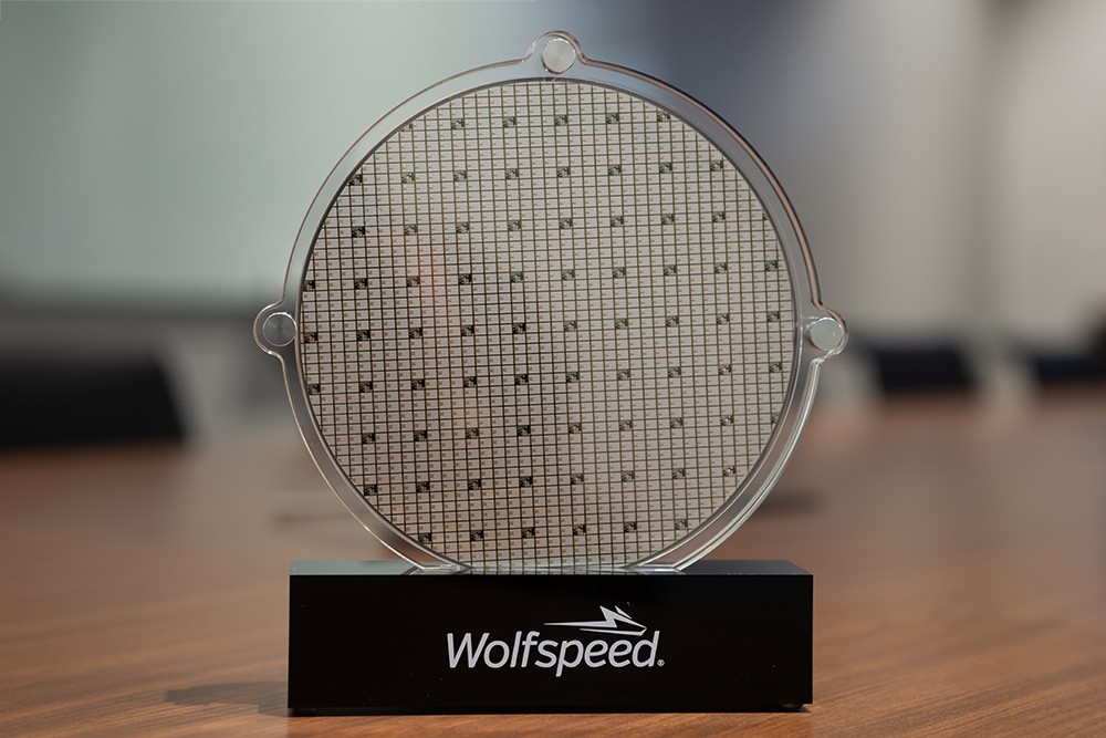
A stock image related to silicon carbide wafer.
In aerospace and defense, SiC wafers are utilized in radar and satellite communication systems due to their resilience in extreme environmental conditions. The ability to operate reliably at high temperatures and under significant stress is critical for mission success. B2B buyers in this sector must ensure that their suppliers have the necessary certifications and experience in aerospace-grade materials to meet the high standards required for safety and reliability.
Related Video: What is Silicon Carbide?
The Problem: B2B buyers often struggle with sourcing silicon carbide (SiC) wafers that meet their specific quality standards. Many suppliers may provide wafers that fail to deliver the required specifications for high-performance applications, such as power electronics or automotive systems. This inconsistency can lead to production delays and increased costs, particularly when the wafers are intended for critical applications in emerging markets like Africa or South America, where supply chain reliability is paramount.
The Solution: To mitigate this sourcing challenge, buyers should establish a robust supplier evaluation process. Begin by assessing suppliers based on their certifications, such as ISO or TS16949, which indicate adherence to quality management standards. Engage in direct communication with potential suppliers to understand their manufacturing processes and quality control measures. Moreover, consider conducting on-site audits or requesting samples before making bulk purchases. Networking through industry forums or associations can also help in identifying reputable suppliers with a proven track record in producing high-quality SiC wafers tailored to your specific needs.
The Problem: Many B2B buyers lack the technical expertise required to fully understand the specifications of silicon carbide wafers, leading to the purchase of inappropriate products for their applications. This is particularly true in regions like the Middle East, where rapidly evolving technology requires constant updates in knowledge. Misunderstandings about parameters such as wafer thickness, doping levels, and crystal orientation can result in suboptimal performance in end products.
The Solution: To address this knowledge gap, organizations should invest in training sessions or workshops that focus on the properties and applications of silicon carbide wafers. Collaborating with industry experts or consultants can provide invaluable insights into the technical aspects of SiC technology. Additionally, consider creating a cross-functional team that includes engineers and procurement specialists to facilitate better communication and understanding of technical requirements. Providing clear documentation and guidelines on the necessary specifications can further streamline the purchasing process and ensure that the correct wafers are sourced.
The Problem: The high cost of silicon carbide wafers can be a significant barrier for businesses, especially startups or companies in developing regions like Colombia or Kenya. These costs often stem from the advanced manufacturing processes and the quality materials required to produce high-performance SiC wafers. This financial burden may deter companies from adopting SiC technology, limiting their competitiveness in the market.
The Solution: To navigate these high costs, buyers should explore collaborative purchasing agreements or group buying options with other companies in similar industries. By pooling resources, businesses can negotiate better pricing with suppliers. Additionally, consider evaluating the total cost of ownership (TCO) rather than just the upfront purchase price. Investing in higher-quality wafers may yield long-term savings through improved efficiency and reduced failure rates. Exploring government incentives or funding programs aimed at promoting advanced manufacturing technologies can also help offset some of the initial investment costs associated with silicon carbide wafers.
When selecting materials for silicon carbide (SiC) wafers, international B2B buyers must consider various factors that influence performance, cost, and suitability for specific applications. The following analysis explores four common materials used in the production of silicon carbide wafers, focusing on their properties, advantages, disadvantages, and implications for buyers, particularly in regions like Africa, South America, the Middle East, and Europe.
Silicon carbide itself is a compound semiconductor known for its high thermal conductivity, exceptional hardness, and resistance to thermal shock. It can withstand high temperatures (up to 1600°C) and has excellent corrosion resistance, making it suitable for harsh environments.
Pros:
- High thermal and electrical conductivity enhances performance in power electronics.
- Excellent mechanical strength increases durability.
Cons:
- Higher manufacturing complexity can lead to increased costs.
- Limited availability in some regions may affect supply chains.
Impact on Application:
SiC wafers are ideal for high-power and high-frequency applications, such as in electric vehicles and renewable energy systems.
Considerations for International Buyers:
Buyers should ensure compliance with international standards such as ASTM and JIS. Availability may vary, so sourcing from established suppliers is crucial.
Sapphire is often used as a substrate for SiC wafers due to its excellent thermal stability and transparency. It can withstand high temperatures and offers good chemical resistance.
Pros:
- High thermal conductivity supports efficient heat dissipation.
- Good mechanical properties enhance wafer durability.
Cons:
- More expensive than traditional substrates like silicon.
- Difficulties in manufacturing can lead to higher costs.
Impact on Application:
Sapphire substrates are beneficial for optoelectronic devices, particularly in LED applications.
Considerations for International Buyers:
Sapphire's high cost may be a deterrent for some buyers. It's essential to evaluate the total cost of ownership when considering this material.
Silicon is a widely used substrate for semiconductor devices, including SiC wafers. It offers good electrical properties and is relatively inexpensive compared to other materials.
Pros:
- Lower cost makes it accessible for various applications.
- Established supply chains facilitate easier procurement.
Cons:
- Lower thermal conductivity compared to SiC and sapphire.
- Limited performance in high-temperature applications.
Impact on Application:
Silicon substrates are suitable for standard electronic devices but may not perform well in high-power applications.
Considerations for International Buyers:
Buyers from emerging markets should consider silicon for cost-sensitive projects, but they must also assess performance requirements carefully.
Gallium nitride is another semiconductor material that can be used in conjunction with silicon carbide. It offers high efficiency and performance in power applications.
Pros:
- Excellent efficiency in high-frequency applications.
- Good thermal stability enhances performance.
Cons:
- Higher cost and complexity in processing.
- Limited availability in some regions.
Impact on Application:
GaN is particularly effective in RF applications and power converters.
Considerations for International Buyers:
Buyers should be aware of the regulatory environment regarding GaN materials in their respective regions, as standards may vary.
| Material | Typical Use Case for silicon carbide wafer | Key Advantage | Key Disadvantage/Limitation | Relative Cost (Low/Med/High) |
|---|---|---|---|---|
| Silicon Carbide | High-power electronics, electric vehicles | High thermal and electrical conductivity | Higher manufacturing complexity | High |
| Sapphire | Optoelectronic devices, LEDs | Excellent thermal stability | More expensive and difficult to manufacture | High |
| Silicon | Standard electronic devices | Lower cost and established supply chains | Lower thermal conductivity | Low |
| Gallium Nitride | RF applications, power converters | Excellent efficiency in high-frequency applications | Higher cost and limited availability | Med |
This guide serves as a strategic resource for international B2B buyers, enabling informed decisions based on material properties, application suitability, and regional considerations.
The manufacturing of silicon carbide (SiC) wafers involves several critical stages that ensure the production of high-quality substrates suitable for various applications, including power electronics and high-frequency devices. The main stages include:
Material Preparation
- Raw Material Selection: The process begins with the selection of high-purity silicon carbide grains, which can be either 3C-SiC, 4H-SiC, or 6H-SiC, depending on the intended application.
- Crystal Growth: The chosen SiC grains undergo a crystal growth process, typically using the Physical Vapor Transport (PVT) method or the Chemical Vapor Deposition (CVD) technique. The PVT method allows for the growth of bulk crystals, while CVD is preferred for high-quality thin films.
Forming the Wafer
- Wafer Slicing: Once the crystal growth is completed, the SiC boule is sliced into thin wafers using diamond wire saws. Precision in slicing is critical to minimize kerf loss and ensure uniform thickness.
- Surface Grinding and Polishing: The sliced wafers are then ground and polished to achieve a smooth surface. This process enhances the wafer’s electrical and optical properties, which are essential for device performance.
Assembly
- Wafer Cleaning: Before any further processing, wafers undergo cleaning to remove any contaminants that may affect subsequent layers and device fabrication.
- Doping: Depending on the application, the wafers may be doped with specific impurities to modify their electrical properties. This is often achieved through ion implantation or diffusion techniques.
Finishing
- Oxidation and Annealing: The wafers may be oxidized to grow a thin layer of silicon dioxide, which serves as an insulating layer. Annealing processes are employed to repair defects and improve the crystal quality.
- Final Inspection: The finished wafers undergo a final inspection to ensure they meet specified standards before shipment.
Quality assurance (QA) in the manufacturing of silicon carbide wafers is vital to ensure reliability and performance. Here are some key QA practices:
Adherence to International Standards
- ISO 9001 Certification: Manufacturers should be ISO 9001 certified, ensuring they follow a quality management system that emphasizes customer satisfaction and continuous improvement.
- Industry-Specific Certifications: Depending on the application, additional certifications such as CE (Conformité Européenne) for products sold in Europe, or API (American Petroleum Institute) for oil and gas applications may be required.
Quality Control Checkpoints
- Incoming Quality Control (IQC): Raw materials and components must be inspected upon arrival to ensure they meet specified quality standards.
- In-Process Quality Control (IPQC): Throughout the manufacturing process, various checkpoints are established to monitor and control the quality of the wafers at different stages.
- Final Quality Control (FQC): A thorough inspection is conducted on the finished wafers to check for defects, surface quality, and dimensional accuracy.
Common Testing Methods for Silicon Carbide Wafers
- Electrical Testing: This includes resistivity measurements and breakdown voltage tests to assess the electrical properties of the wafers.
- Optical Inspection: Techniques such as photoluminescence and surface roughness measurements are used to evaluate the wafer's surface quality.
- Mechanical Testing: Wafer strength and durability are assessed through various mechanical tests to ensure they can withstand subsequent processing and application stresses.
International B2B buyers, particularly from regions like Africa, South America, the Middle East, and Europe, should take several steps to verify the quality control practices of silicon carbide wafer suppliers:
Conduct Supplier Audits
- Regular audits can help assess the supplier's compliance with established quality standards and their internal processes. This may include evaluating their manufacturing capabilities, equipment, and quality management systems.
Request Quality Assurance Reports
- Buyers should request detailed QA reports that outline the quality control procedures, testing results, and any certifications held by the supplier. These reports provide insight into the supplier's commitment to quality.
Engage Third-Party Inspection Services
- Utilizing third-party inspection services can provide an objective assessment of the supplier's products. These services can verify compliance with international standards and specific buyer requirements.
International buyers must navigate various nuances when it comes to quality control and certification for silicon carbide wafers:
Understanding Regional Standards
- Different regions may have specific regulatory requirements and standards. Buyers should familiarize themselves with the standards applicable in their respective markets to ensure compliance.
Cultural Considerations
- There may be cultural differences in how quality is perceived and enforced. Buyers should establish clear communication channels with suppliers to ensure mutual understanding of quality expectations.
Documentation and Traceability
- Ensure that suppliers maintain thorough documentation of their manufacturing and quality control processes. This traceability is essential for verifying compliance and addressing any potential quality issues that may arise post-purchase.
By understanding the manufacturing processes and quality assurance practices associated with silicon carbide wafers, B2B buyers can make informed decisions and foster successful partnerships with reliable suppliers.
In this sourcing guide, we aim to provide international B2B buyers, particularly those from Africa, South America, the Middle East, and Europe, with a clear and actionable checklist for procuring silicon carbide wafers. Understanding the nuances of this material and the procurement process is essential to ensure you meet your specific technical requirements while establishing reliable supplier relationships.
Before initiating the sourcing process, clearly outline the technical specifications of the silicon carbide wafers you need. Consider factors such as diameter, thickness, crystal orientation, and doping type. This clarity will not only streamline your search but will also help suppliers provide you with accurate quotes and relevant products.
Conduct thorough research to identify potential suppliers of silicon carbide wafers. Look for manufacturers with a proven track record in the semiconductor industry and those who specialize in silicon carbide products. Utilize industry directories, trade shows, and online platforms to gather a list of candidates.
Before moving forward with any supplier, verify their certifications. Look for ISO 9001 and other relevant quality management certifications, which indicate adherence to international quality standards. Certification ensures that the supplier maintains consistent quality and can meet your technical specifications.
Once you have shortlisted potential suppliers, request samples of their silicon carbide wafers. This allows you to assess the quality and verify that the product meets your specifications. Additionally, ask for detailed technical data sheets that outline the wafer’s properties, including resistivity, surface roughness, and any other relevant parameters.
After evaluating samples, request formal quotes from your shortlisted suppliers. Compare pricing structures, keeping in mind that the lowest price may not always equate to the best value. Additionally, clarify payment terms, such as upfront deposits, credit terms, and any potential discounts for bulk purchases.
Understanding the logistics of shipping is crucial. Discuss delivery timelines, shipping methods, and costs with your suppliers. Ensure they have reliable logistics partners to avoid delays that could impact your production schedule.
Once you’ve selected a supplier, establish a communication plan to facilitate ongoing interactions. Clear communication helps in addressing any potential issues quickly and ensures that both parties remain aligned on expectations and requirements.
By following this checklist, B2B buyers can navigate the complexities of sourcing silicon carbide wafers more effectively, ensuring that they make informed decisions that align with their technical needs and business objectives.
Understanding the cost structure of silicon carbide (SiC) wafers is essential for B2B buyers, particularly those in Africa, South America, the Middle East, and Europe. The main components that contribute to the total cost include:
Materials: The primary cost driver in SiC wafer production is the raw materials. High-purity silicon carbide crystals are required, and the price can fluctuate based on market demand and sourcing challenges.
Labor: Skilled labor is necessary for the manufacturing process, including both production and quality control. Labor costs can vary significantly depending on the location of the manufacturing facility.
Manufacturing Overhead: This includes expenses related to facility maintenance, utilities, and equipment depreciation. The efficiency of the manufacturing process can influence these costs.
Tooling: The initial setup for wafer production often requires specialized tooling, which can be a significant upfront cost. This is particularly relevant for custom specifications.
Quality Control (QC): Ensuring that wafers meet specific performance standards requires rigorous testing and quality assurance protocols, adding to the overall cost.
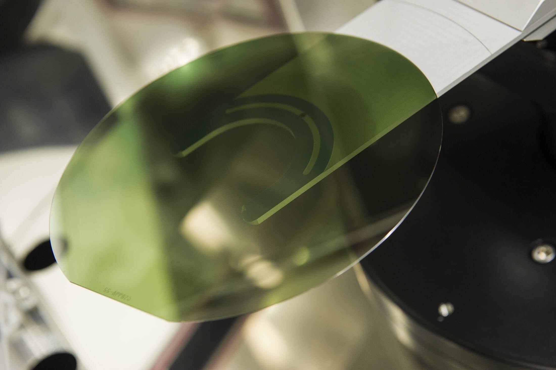
A stock image related to silicon carbide wafer.
Logistics: Transportation costs for raw materials and finished wafers can vary based on geographic location and shipping terms. This is especially critical for international buyers who must consider import duties and tariffs.
Margin: Suppliers often build a profit margin into the pricing structure, which can vary based on competition and market conditions.
Several factors influence the pricing of silicon carbide wafers, making it essential for buyers to consider these elements during procurement:
Volume and Minimum Order Quantity (MOQ): Larger orders typically result in lower per-unit costs due to economies of scale. Understanding the supplier's MOQ can help in negotiating better pricing.
Specifications and Customization: Custom specifications, such as diameter, thickness, and doping levels, can significantly impact the price. Standard wafers are generally cheaper than customized options.
Material Quality and Certifications: Higher quality wafers that meet specific industry certifications (such as ISO) may come at a premium. Buyers must assess the importance of certification against their application needs.
Supplier Factors: The reputation and reliability of the supplier can also influence pricing. Established suppliers may charge more due to their quality assurance processes and track record.
Incoterms: The agreed-upon Incoterms can affect total costs, including responsibilities for shipping, insurance, and tariffs. Understanding these terms can lead to better cost management.
International B2B buyers should adopt several strategies to enhance cost efficiency in silicon carbide wafer sourcing:
Negotiate Terms: Engage suppliers in discussions around pricing, payment terms, and delivery schedules. Building a long-term relationship may yield better pricing over time.
Evaluate Total Cost of Ownership (TCO): Consider all associated costs, including logistics and potential delays, when assessing the price of wafers. A lower initial price may not always equate to a better deal.
Research Market Trends: Stay informed about market dynamics and pricing trends in the semiconductor industry. This knowledge can provide leverage during negotiations.
Leverage Bulk Buying: If possible, consolidate purchases with other companies to meet MOQs. This can lead to lower prices per unit.
Assess Supplier Location: Consider sourcing from suppliers closer to your region to minimize shipping costs and lead times, particularly for urgent projects.
While sourcing silicon carbide wafers, understanding the intricate cost structure and price influencers can empower buyers to make informed purchasing decisions. By employing effective negotiation tactics and focusing on total cost considerations, international B2B buyers can optimize their procurement processes and achieve better value.
When considering semiconductor solutions, silicon carbide (SiC) wafers have gained significant traction due to their superior thermal and electrical properties. However, it's essential for B2B buyers, especially in emerging markets such as Africa, South America, the Middle East, and Europe, to evaluate alternatives that may align better with their specific needs, budget constraints, or application requirements. This section compares silicon carbide wafers with two viable alternatives: gallium nitride (GaN) wafers and traditional silicon wafers.
| Comparison Aspect | Silicon Carbide Wafer | Gallium Nitride Wafer | Traditional Silicon Wafer |
|---|---|---|---|
| Performance | High efficiency, superior thermal conductivity, ideal for high-voltage applications | Excellent high-frequency performance, lower on-resistance | Lower efficiency, suitable for low-power applications |
| Cost | Higher initial cost due to material and processing | Moderate cost, but can be more expensive than SiC in some applications | Generally lower cost, widely available |
| Ease of Implementation | Requires specialized equipment and knowledge | Similar to SiC but slightly easier due to existing processes | Easy implementation, standard processes in use |
| Maintenance | Low maintenance, robust in extreme conditions | Low maintenance, but sensitive to temperature variations | Moderate maintenance, standard reliability |
| Best Use Case | High-power, high-temperature applications (e.g., EVs, industrial) | RF and power electronics, LED applications | Consumer electronics, low-power devices |
Gallium nitride (GaN) wafers are increasingly popular in power electronics and RF applications. They boast excellent performance at high frequencies and temperatures, making them ideal for applications like wireless charging, RF amplifiers, and high-efficiency power converters. The primary advantage of GaN is its ability to operate at higher voltages and temperatures than traditional silicon, leading to better efficiency. However, GaN can be more expensive than SiC in specific scenarios, particularly in high-power applications.
Traditional silicon wafers have been the cornerstone of semiconductor manufacturing for decades. They are widely available and cost-effective, making them suitable for low-power consumer electronics. While they do not offer the same performance as SiC or GaN in high-voltage or high-frequency applications, their ease of implementation and well-established manufacturing processes make them a reliable choice for many applications. However, as technology advances, traditional silicon may struggle to keep pace with the growing demands for efficiency and power handling.
Selecting the appropriate semiconductor wafer technology depends on various factors, including the specific application, performance requirements, and budget constraints. For high-power and high-temperature applications, silicon carbide wafers offer unmatched performance, making them a worthwhile investment despite the higher initial costs. On the other hand, gallium nitride wafers may be preferable for applications requiring high-frequency performance but at a slightly lower thermal threshold. Traditional silicon wafers remain a solid choice for cost-sensitive, low-power applications.
Ultimately, B2B buyers should assess their unique operational needs and long-term goals, considering factors such as scalability, technology roadmap, and total cost of ownership when making their decision.
When sourcing silicon carbide wafers, international B2B buyers should familiarize themselves with essential technical properties and trade terminology. This knowledge not only aids in making informed purchasing decisions but also facilitates smoother negotiations and transactions across diverse markets, including Africa, South America, the Middle East, and Europe.
Silicon carbide wafers come in various material grades, which indicate their purity and crystalline structure. Higher-grade wafers, such as 4H-SiC and 6H-SiC, are preferred for high-performance applications due to their superior electrical and thermal properties. Understanding the material grade is crucial for buyers to ensure they are purchasing wafers that meet the specific requirements of their applications, particularly in power electronics and high-frequency devices.
The diameter of silicon carbide wafers typically ranges from 2 inches to 6 inches or more. Larger diameters can lead to increased yield and reduced costs per unit for manufacturers. For B2B buyers, selecting the appropriate wafer diameter is essential, as it directly impacts the scale of production and the compatibility with existing fabrication processes.
Tolerance refers to the allowable deviation from specified dimensions, while flatness indicates the wafer's surface uniformity. Both specifications are critical for ensuring the wafer fits precisely in processing equipment and maintains consistent performance during manufacturing. Buyers should prioritize wafers with tight tolerances and superior flatness to minimize defects and improve overall yield.
Doping involves introducing impurities into silicon carbide to modify its electrical properties. The concentration of dopants (e.g., nitrogen for n-type or aluminum for p-type) affects the wafer's conductivity and is pivotal for applications in semiconductor devices. Buyers need to specify the required doping concentration to ensure compatibility with their intended applications, particularly in power devices and RF applications.
The surface finish of silicon carbide wafers can significantly influence the performance of subsequent processing steps. A polished or epitaxial surface finish is often necessary for high-frequency and high-power applications. Buyers should assess the surface finish specifications to ensure they align with the requirements of their fabrication processes.
OEM refers to companies that produce products or components that are used in another company's end products. In the context of silicon carbide wafers, OEMs are critical partners for buyers looking to integrate wafers into larger systems or devices. Understanding OEM relationships can help buyers negotiate better pricing and service terms.
MOQ is the minimum number of units a supplier is willing to sell in a single order. This term is vital for buyers to understand as it affects budgeting and inventory management. B2B buyers should inquire about MOQs to ensure they can meet production needs without overcommitting to unnecessary inventory.
An RFQ is a document issued by buyers to solicit price quotes from suppliers for specific products or services. In the silicon carbide wafer market, issuing an RFQ can help buyers compare pricing, terms, and availability from multiple suppliers, ensuring they make informed purchasing decisions.
Incoterms are a set of predefined commercial terms published by the International Chamber of Commerce that clarify the responsibilities of buyers and sellers in international trade. Understanding Incoterms is crucial for B2B buyers as they dictate the costs, risks, and logistics involved in the transportation of silicon carbide wafers.
Lead time refers to the time taken from placing an order to receiving the product. For silicon carbide wafers, lead times can vary based on production capabilities and demand. Buyers should factor lead times into their planning to ensure timely delivery and avoid disruptions in their manufacturing processes.
By comprehensively understanding these technical properties and trade terms, international B2B buyers can navigate the silicon carbide wafer market more effectively, ensuring they make strategic purchasing decisions that align with their operational needs.
The silicon carbide (SiC) wafer market is experiencing significant growth, driven by increasing demand for energy-efficient solutions in various sectors, including automotive, telecommunications, and renewable energy. This growth is largely attributed to the global shift toward electric vehicles (EVs) and the need for efficient power electronics. As international B2B buyers from regions like Africa, South America, the Middle East, and Europe look to source silicon carbide wafers, understanding these market dynamics is crucial.
Emerging trends in the silicon carbide wafer sector include advancements in manufacturing technologies that enhance yield and reduce costs. Companies are increasingly adopting vertical integration strategies to control supply chains and improve product quality. Additionally, the rise of wide bandgap semiconductors is encouraging investment in R&D, aiming for higher efficiency and performance in power devices. Buyers should be aware of the competitive landscape, as established players and new entrants are continually innovating to capture market share.
Another noteworthy trend is the geographical shift in manufacturing hubs. While traditional markets in Europe and North America remain strong, there is a growing interest in establishing production facilities in Asia and other emerging markets. This shift presents opportunities for buyers to negotiate better pricing and terms, particularly as local production increases.
Sustainability is becoming a paramount concern in the silicon carbide wafer sector. The environmental impact of SiC wafer production, particularly in terms of energy consumption and waste generation, is under scrutiny. Buyers are increasingly prioritizing suppliers that demonstrate a commitment to sustainable practices, including the use of renewable energy sources and responsible waste management.
Ethical sourcing is another critical factor. International buyers are looking for suppliers that adhere to rigorous ethical standards throughout their supply chains. This includes ensuring that raw materials are sourced responsibly and that labor practices meet international human rights standards. Certifications such as ISO 14001 for environmental management and ISO 45001 for occupational health and safety are becoming essential for suppliers aiming to attract conscientious buyers.
Moreover, the demand for "green" silicon carbide materials is on the rise. Innovations in production processes that reduce carbon footprints and increase recycling rates are gaining traction. Buyers should seek partnerships with manufacturers that not only provide high-quality silicon carbide wafers but also demonstrate a commitment to sustainability and ethical sourcing.
The evolution of silicon carbide wafers can be traced back to the early 20th century when SiC was first synthesized. However, it wasn’t until the late 1990s and early 2000s that advancements in crystal growth techniques, such as the physical vapor transport method, enabled the production of high-quality SiC wafers suitable for commercial applications.
As demand for efficient power devices surged, particularly with the advent of electric vehicles and renewable energy systems, silicon carbide wafers began to gain prominence. The material’s superior thermal conductivity and electric field breakdown strength made it ideal for high-performance applications. Today, silicon carbide wafers are seen as a critical component in the shift toward more sustainable technologies, providing B2B buyers with not only high performance but also a pathway to lower environmental impact.
In conclusion, understanding the market dynamics, sustainability considerations, and the historical context of silicon carbide wafers is vital for international B2B buyers. By aligning sourcing strategies with these insights, companies can effectively navigate the evolving landscape of the silicon carbide sector.
1. How do I choose the right silicon carbide wafer supplier?
Selecting the right silicon carbide wafer supplier involves several key considerations. Start by assessing the supplier’s experience and expertise in the industry. Look for certifications and quality assurances that indicate compliance with international standards, such as ISO or RoHS. Additionally, evaluate their production capacity and technology used to ensure they can meet your specific requirements. It's also beneficial to request samples or technical data sheets to gauge the quality of their products before making a commitment.
2. What are the typical applications of silicon carbide wafers?
Silicon carbide wafers are widely used in high-performance applications, including power electronics, RF devices, and high-temperature environments. They are particularly valuable in electric vehicles, solar inverters, and industrial power supplies due to their efficiency and thermal conductivity. Understanding the specific application requirements, such as voltage ratings and thermal management, will help you select the appropriate type of silicon carbide wafer for your project.
3. What are the minimum order quantities (MOQ) for silicon carbide wafers?
Minimum order quantities for silicon carbide wafers can vary significantly among suppliers, often ranging from a few pieces to several hundred. Factors influencing MOQ include the supplier's production capabilities, the type of wafers required, and customization options. It is advisable to discuss your specific needs with potential suppliers to negotiate favorable terms that align with your procurement strategy.
4. How can I customize silicon carbide wafers to meet my specifications?
Customization of silicon carbide wafers can include alterations in size, thickness, doping levels, and surface finish. Most suppliers will work with you to understand your precise requirements and may offer tailored solutions based on your application needs. Ensure you provide detailed specifications and communicate regularly with the supplier throughout the design and production process to achieve the desired results.
5. What payment terms should I expect when purchasing silicon carbide wafers internationally?
Payment terms for international purchases of silicon carbide wafers typically range from upfront payments to net 30 or net 60 terms, depending on the supplier's policies and your negotiation skills. Common methods include wire transfers, letters of credit, or payment through trade platforms. Be sure to clarify payment expectations and any potential additional costs, such as customs duties or shipping fees, to avoid surprises.
6. How do I ensure quality assurance for silicon carbide wafers?
To ensure quality assurance when sourcing silicon carbide wafers, request documentation of the supplier's quality control processes, including certifications and test results. Look for suppliers who conduct rigorous testing at various production stages, such as material composition, surface integrity, and electrical properties. Establishing a clear quality agreement that outlines your expectations can also help mitigate risks and ensure you receive the product quality required for your applications.
7. What logistics considerations should I take into account when sourcing silicon carbide wafers?
Logistics is a crucial factor in sourcing silicon carbide wafers, especially for international buyers. Consider shipping times, customs clearance processes, and costs associated with transportation. It is advisable to work with suppliers who have experience in international shipping and can provide insight into potential delays or challenges. Additionally, ensure that the packaging is suitable for protecting fragile wafers during transit to prevent damage.
8. How can I vet suppliers of silicon carbide wafers effectively?
Vetting suppliers of silicon carbide wafers involves a thorough evaluation of their credentials, reputation, and customer reviews. Start by checking their industry experience and references from previous clients. Conduct background checks to ensure they have a solid financial standing and comply with relevant regulations. Additionally, visiting the supplier's facilities, if feasible, can provide deeper insights into their manufacturing processes and quality control practices.
The information provided in this guide, including content regarding manufacturers, technical specifications, and market analysis, is for informational and educational purposes only. It does not constitute professional procurement advice, financial advice, or legal advice.
While we have made every effort to ensure the accuracy and timeliness of the information, we are not responsible for any errors, omissions, or outdated information. Market conditions, company details, and technical standards are subject to change.
B2B buyers must conduct their own independent and thorough due diligence before making any purchasing decisions. This includes contacting suppliers directly, verifying certifications, requesting samples, and seeking professional consultation. The risk of relying on any information in this guide is borne solely by the reader.
In the evolving landscape of silicon carbide wafer sourcing, strategic procurement is essential for international B2B buyers aiming to capitalize on the growing demand for high-performance semiconductor materials. Buyers from regions such as Africa, South America, the Middle East, and Europe must prioritize establishing robust supplier relationships to secure competitive pricing and ensure product quality. Understanding regional market dynamics and technological advancements will empower these buyers to make informed decisions.
What are the key advantages of strategic sourcing for silicon carbide wafers? By leveraging strategic sourcing, businesses can reduce costs, mitigate supply chain risks, and enhance innovation capabilities. Furthermore, engaging with suppliers who are at the forefront of technological advancements ensures access to cutting-edge materials that can drive product performance and sustainability.
Looking ahead, the silicon carbide market is poised for significant growth, driven by increased demand in electric vehicles, renewable energy, and advanced electronics. B2B buyers are encouraged to actively engage in strategic sourcing initiatives, explore diverse supplier networks, and remain adaptable to market changes. Embrace the opportunities that lie ahead and position your business as a leader in the silicon carbide value chain.
Tags: Black Silicon Carbide, White Fused Alumina, Brown Fused Alumina, Pink Fused Alumina, Black Fused Alumina