The global demand for silicon carbide (SiC) wafers is rapidly accelerating, driven by their pivotal role in high-performance electronics, electric vehicles, renewable energy systems, and advanced industrial applications. For international B2B buyers—especially those in Africa, South America, the Middle East, and Europe—sourcing reliable SiC wafer suppliers is not just a procurement task but a strategic decision that directly impacts product quality, innovation potential, and competitive advantage.
Navigating this complex market requires deep insight into the varied types of SiC wafers available, including differences in polytypes, diameters, and surface finishes. Understanding the nuances of raw materials and manufacturing processes is equally critical to ensure consistency and yield. Moreover, quality control standards and certifications vary widely among suppliers, influencing both the performance and reliability of end products.
This guide offers a comprehensive roadmap tailored for global buyers aiming to make informed sourcing decisions. It covers everything from wafer specifications and manufacturing best practices to supplier evaluation criteria, cost considerations, and current market trends. Additionally, it addresses frequently asked questions that help clarify technical and logistical challenges unique to international trade.
By leveraging this resource, B2B buyers from diverse regions can confidently identify and partner with the right SiC wafer suppliers who meet their exacting standards. The insights provided empower procurement teams to optimize supply chains, reduce risks, and foster innovation—ultimately driving business growth in an increasingly competitive global landscape.
Illustrative Image (Source: Google Search)
| Type Name | Key Distinguishing Features | Primary B2B Applications | Brief Pros & Cons for Buyers |
|---|---|---|---|
| Bulk SiC Wafer Suppliers | Large-scale production, standardized sizes and grades | Power electronics, automotive, industrial | + Cost-effective for high volume – Limited customization |
| Specialty SiC Wafer Makers | Custom doping, unique crystal orientations, niche specifications | High-frequency devices, RF components, sensors | + Tailored solutions – Higher cost, longer lead times |
| Foundry-Integrated Suppliers | Combine wafer supply with semiconductor fabrication services | OEMs needing turnkey solutions | + Streamlined supply chain – Less flexibility in sourcing |
| High-Purity SiC Suppliers | Ultra-low defect density, high crystalline quality | Aerospace, defense, advanced research | + Superior performance – Premium pricing, smaller batches |
| Regional/Niche Market Suppliers | Focus on specific geographic markets or specialized sectors | Localized industrial applications, emerging markets | + Local support, reduced logistics – May lack global scale |
Bulk SiC Wafer Suppliers
These suppliers focus on mass-producing silicon carbide wafers with standardized sizes and doping levels. Their strength lies in economies of scale, making them ideal for B2B buyers in automotive, industrial power electronics, and renewable energy sectors who require consistent quality at competitive prices. Buyers should evaluate volume discounts, delivery reliability, and certification standards. However, customization options are often limited, which may restrict innovation for specialized applications.
Specialty SiC Wafer Makers
Specialty suppliers offer wafers with custom doping, crystal orientations, and unique specifications tailored for high-frequency and RF devices or sensor technologies. These suppliers cater to B2B buyers prioritizing performance and differentiation, such as telecom equipment manufacturers or precision instrumentation firms. While the flexibility in specifications is advantageous, buyers must consider longer lead times and higher costs, balancing innovation needs against budget constraints.
Foundry-Integrated Suppliers
These suppliers provide a combined package of SiC wafer supply and semiconductor fabrication services, appealing to OEMs seeking streamlined operations and reduced supplier complexity. This integration supports faster time-to-market for products requiring both wafer and device manufacturing. B2B buyers benefit from simplified logistics and quality control but may face less sourcing flexibility and potential dependency on a single supplier ecosystem.
High-Purity SiC Suppliers
Focused on delivering wafers with ultra-low defect densities and exceptional crystalline quality, these suppliers serve advanced sectors such as aerospace, defense, and cutting-edge research institutions. Buyers in these areas prioritize wafer performance and reliability over cost, making premium pricing acceptable. Purchasing decisions should include thorough evaluation of defect metrics, traceability, and supplier certifications to ensure compliance with stringent industry standards.
Regional/Niche Market Suppliers
These suppliers specialize in serving specific geographic regions or niche industrial sectors, offering localized support and potentially faster delivery times. They are particularly relevant for B2B buyers in emerging markets or industries with unique regulatory or environmental requirements. While regional suppliers can enhance supply chain resilience and reduce logistics costs, buyers should assess their capacity to scale and the consistency of quality against global competitors.
Related Video: microDICE - Wafer dicing system for SiC
| Industry/Sector | Specific Application of sic wafer suppliers | Value/Benefit for the Business | Key Sourcing Considerations for this Application |
|---|---|---|---|
| Power Electronics | High-efficiency power devices for electric vehicles (EVs) | Enhanced energy efficiency and thermal management reduces costs and improves reliability | Consistent wafer quality, thermal conductivity, and supplier capacity for volume orders |
| Renewable Energy | Silicon carbide wafers for photovoltaic inverters | Increased inverter efficiency and durability under harsh conditions | Wafer purity, defect density, and long-term supply stability |
| Telecommunications | RF and microwave devices for 5G infrastructure | Superior frequency performance and reduced signal loss | High-frequency performance specs, wafer uniformity, and lead times |
| Aerospace & Defense | High-temperature and radiation-resistant electronics | Reliable operation in extreme environments, critical for mission success | Compliance with stringent quality and certification standards |
| Industrial Automation | High-voltage, high-power semiconductor devices | Improved system efficiency and operational lifespan | Custom wafer specifications, robust supplier technical support |
Silicon carbide (SiC) wafers are pivotal in manufacturing power electronic devices used in electric vehicles, such as inverters and power modules. These wafers enable higher switching frequencies and better thermal performance compared to traditional silicon, which translates into smaller, lighter, and more efficient powertrain components. For international B2B buyers in regions like Europe and the Middle East, prioritizing wafer consistency and thermal conductivity is critical to meet stringent automotive standards and support large-scale EV production.
SiC wafers are increasingly used in photovoltaic (PV) inverter systems to convert DC from solar panels into AC electricity efficiently. Their ability to operate at higher voltages and temperatures ensures improved inverter reliability and efficiency, which is essential for solar farms in Africa and South America where environmental conditions can be challenging. Buyers should focus on wafer purity and defect density to guarantee inverter longevity and performance, alongside securing suppliers who can assure stable long-term supply.
The rollout of 5G networks demands high-frequency RF and microwave components that can handle increased data rates and signal integrity. SiC wafers facilitate the production of these components by offering superior electron mobility and thermal stability. For telecommunications companies in Europe and the Middle East, sourcing wafers with tight uniformity and high-frequency performance parameters is vital. Lead times and supplier responsiveness also impact project timelines in this fast-evolving sector.
In aerospace and defense, SiC wafers are essential for fabricating electronics that must withstand extreme temperatures, radiation, and mechanical stress. These wafers enable the development of high-reliability power modules and sensors critical for mission success. Buyers from regions like Europe and the Middle East must ensure suppliers comply with rigorous certification standards and quality assurance processes, as well as provide traceability and documentation to meet defense procurement requirements.
SiC wafers are used to produce high-voltage, high-power semiconductor devices that drive industrial automation systems, including robotics and motor controls. These devices benefit from SiC’s superior efficiency and durability, leading to reduced downtime and maintenance costs. International buyers should seek suppliers capable of delivering custom wafer specifications and strong technical support to tailor solutions for diverse industrial environments, particularly in emerging markets such as Africa and South America.
Related Video: Silicon Wafer Production
Silicon carbide (SiC) wafers are critical components in power electronics, sensors, and high-temperature devices, making material selection a strategic decision for B2B buyers worldwide. Understanding the common materials used in SiC wafer production, their properties, and regional compliance considerations is essential for optimizing supply chain decisions and ensuring product performance.
Key Properties:
4H-SiC is the most widely used polytype for SiC wafers due to its wide bandgap (~3.26 eV), high electron mobility, and excellent thermal conductivity (~4.9 W/cm·K). It offers high breakdown electric field strength and can operate reliably at temperatures exceeding 600°C, making it ideal for high-power and high-frequency applications.
Pros & Cons:
- Pros: Superior electrical performance, excellent thermal stability, and well-established manufacturing processes.
- Cons: Higher production complexity and cost compared to other polytypes; requires precise control during crystal growth to minimize defects.
Impact on Application:
4H-SiC wafers are preferred for power devices such as MOSFETs and Schottky diodes, especially in automotive, renewable energy, and industrial sectors where efficiency and thermal management are critical.
International B2B Considerations:
Buyers from Europe (e.g., France) and the Middle East often prioritize compliance with ASTM standards (e.g., ASTM F1857 for SiC wafers) and ISO certifications for quality assurance. African and South American buyers should verify supplier adherence to these standards and consider logistics for handling sensitive wafers. Australia’s growing renewable energy market demands wafers with high reliability, favoring 4H-SiC despite its premium cost.
Key Properties:
6H-SiC has a slightly smaller bandgap (~3.0 eV) and lower electron mobility than 4H-SiC but offers good mechanical strength and thermal conductivity. It is stable at high temperatures and has a hexagonal crystal structure conducive to certain niche applications.
Pros & Cons:
- Pros: Generally lower cost than 4H-SiC, easier to manufacture with fewer defects, and suitable for high-temperature sensors.
- Cons: Inferior electrical performance for power devices, limiting its use in high-frequency or high-efficiency applications.
Impact on Application:
6H-SiC wafers are commonly used in high-temperature sensors, microwave devices, and some optoelectronic applications where electrical performance is less critical but thermal and mechanical stability is essential.
International B2B Considerations:
Buyers in South America and Africa may find 6H-SiC wafers a cost-effective option for industrial sensors and niche electronics. Ensuring suppliers comply with regional standards like DIN (Germany) or JIS (Japan) can facilitate integration into global supply chains. The Middle East’s expanding petrochemical industry values 6H-SiC’s corrosion resistance and temperature tolerance.
Key Properties:
Epitaxial SiC involves growing a thin, high-purity SiC layer atop a SiC substrate, enhancing carrier mobility and reducing defects. This material is crucial for advanced device fabrication, offering superior surface quality and electrical characteristics.
Pros & Cons:
- Pros: Enables high-performance device fabrication with reduced lattice defects, customizable doping profiles, and excellent surface uniformity.
- Cons: Significantly higher manufacturing complexity and cost; requires sophisticated equipment and expertise.
Impact on Application:
Epi-SiC wafers are indispensable for cutting-edge power electronics, RF devices, and high-temperature sensors demanding ultra-high purity and performance.
International B2B Considerations:
European buyers, particularly in France and Germany, often require epi-SiC wafers that meet stringent quality certifications (e.g., SEMI standards). Buyers from Australia and the Middle East should consider suppliers’ capabilities in delivering consistent epitaxial layers to support advanced manufacturing. Importers in Africa and South America need to assess the cost-benefit ratio given the premium pricing and application specificity.
Key Properties:
Polycrystalline SiC consists of multiple small crystals rather than a single crystal structure. It exhibits good thermal conductivity and mechanical strength but has lower electron mobility and higher defect density compared to single-crystal SiC.
Pros & Cons:
- Pros: Lower cost and simpler manufacturing processes; suitable for abrasive, refractory, and structural applications.
- Cons: Not suitable for high-performance electronic devices due to electrical inconsistencies and grain boundary effects.
Impact on Application:
Poly-SiC is often used in substrate materials for mechanical components, heating elements, and protective coatings rather than active semiconductor devices.
International B2B Considerations:
Buyers focused on industrial applications in Africa and South America may prefer poly-SiC for cost-sensitive projects. Compliance with ASTM and ISO standards remains important to ensure material reliability. European buyers may use poly-SiC for non-electronic applications or as a base material for further processing.
| Material | Typical Use Case for sic wafer suppliers | Key Advantage | Key Disadvantage/Limitation | Relative Cost (Low/Med/High) |
|---|---|---|---|---|
| 4H-Silicon Carbide (4H-SiC) | High-power and high-frequency power devices (MOSFETs, diodes) | Superior electrical and thermal performance | High production complexity and cost | High |
| 6H-Silicon Carbide (6H-SiC) | High-temperature sensors, microwave devices | Lower cost, good mechanical and thermal stability | Lower electrical performance limits applications | Medium |
| Epitaxial Silicon Carbide (Epi-SiC) | Advanced power electronics, RF devices | Ultra-high purity and surface quality | Very high manufacturing complexity and cost | High |
| Polycrystalline Silicon Carbide (Poly-SiC) | Industrial components, refractory materials | Cost-effective, robust mechanical properties | Unsuitable for high-performance electronics | Low |
This guide equips international B2B buyers with a clear understanding of material options for SiC wafers, enabling informed procurement decisions aligned with regional standards, application requirements, and budget constraints.
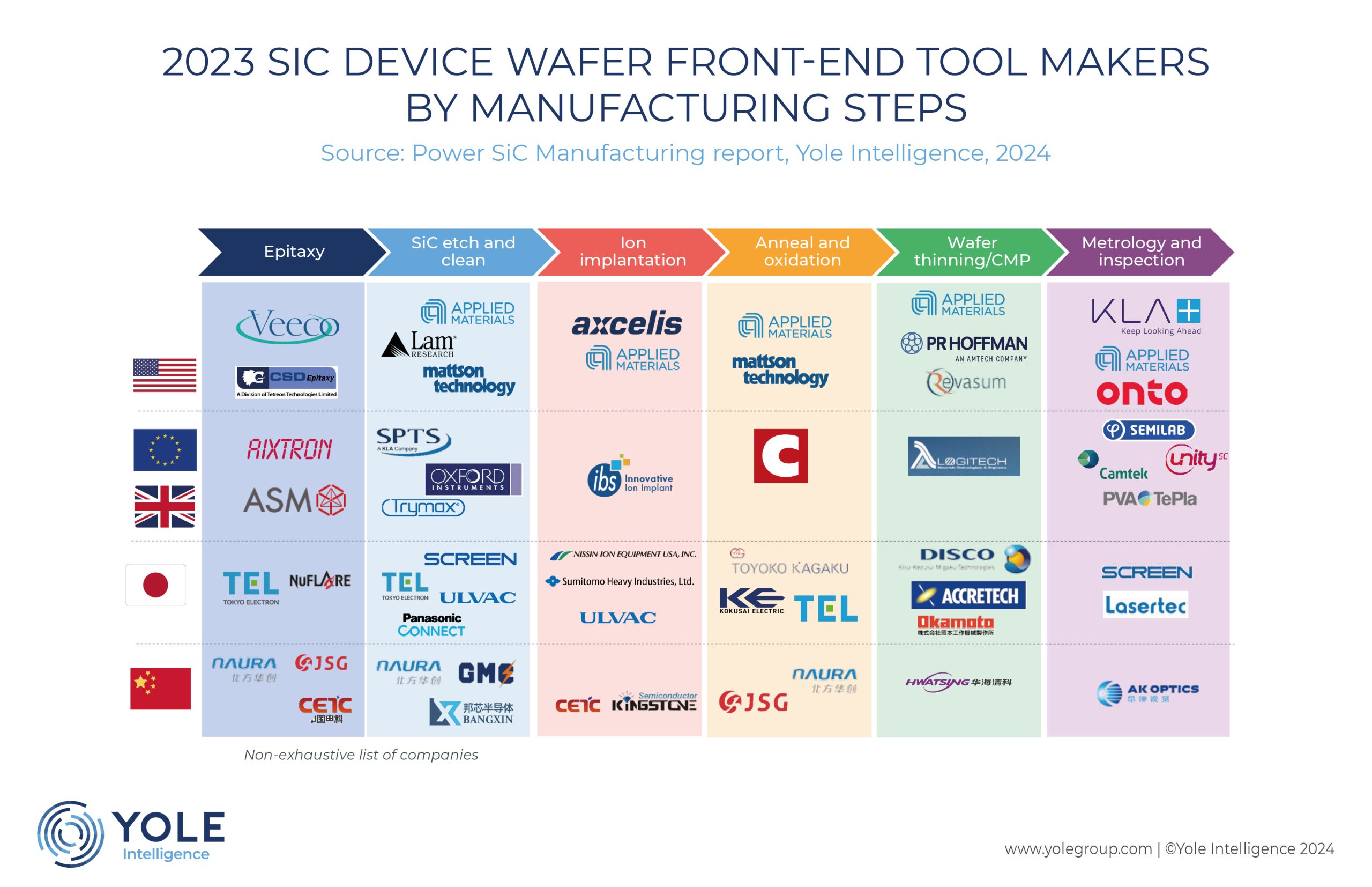
Silicon carbide (SiC) wafers are critical components in high-performance power electronics, favored for their superior thermal conductivity, high breakdown voltage, and efficiency in harsh environments. Understanding the manufacturing process enables B2B buyers to assess supplier capabilities and ensure product consistency.
Key Manufacturing Stages:
Material Preparation:
The process begins with sourcing high-purity raw materials, primarily silicon and carbon. These are combined in a controlled environment to synthesize SiC powder, which serves as the base material. Suppliers typically use chemical vapor deposition (CVD) or physical vapor transport (PVT) methods to grow SiC crystals. Buyers should inquire about the purity levels and traceability of raw materials, as impurities directly affect wafer quality.
Crystal Growth and Forming:
SiC crystals are grown into boules using the PVT technique, where powdered SiC sublimates and recrystallizes on a seed crystal at high temperatures (around 2500°C). This stage demands precise temperature and environment control to minimize defects such as micropipes and dislocations. Suppliers with advanced crystal growth furnaces and real-time monitoring systems tend to produce higher-quality wafers.
Wafer Slicing and Lapping:
The boules are sliced into thin wafers using diamond wire saws. Post slicing, wafers undergo lapping and grinding to achieve the desired thickness and flatness. This stage is critical for surface integrity, as surface damage can degrade device performance. Buyers should verify if suppliers employ automated equipment with fine control to ensure uniform wafer thickness and minimize subsurface damage.
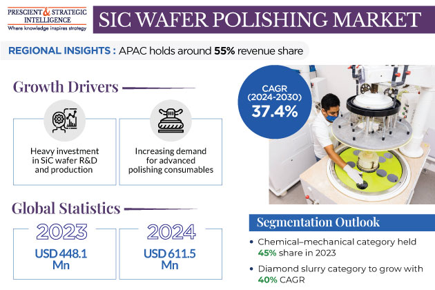
Polishing and Cleaning:
Polishing removes surface irregularities and prepares wafers for device fabrication. Chemical-mechanical polishing (CMP) is commonly used to achieve nanometer-scale surface roughness. After polishing, wafers are cleaned in ultra-pure water and chemical solutions to eliminate contaminants. Buyers should confirm the use of cleanroom environments (ISO Class 5 or better) during this phase to prevent particulate contamination.
Inspection and Packaging:
Finished wafers undergo visual and automated optical inspections to detect defects such as cracks, pits, and contamination. They are then packaged in specialized carriers that protect against mechanical damage and static discharge during shipping. For international buyers, packaging standards must comply with international shipping regulations to prevent damage during transit.
Illustrative Image (Source: Google Search)
Quality assurance (QA) is paramount in SiC wafer production due to the wafers’ role in mission-critical electronic devices. Suppliers adhering to international and industry-specific standards provide greater confidence in product reliability.
Relevant Quality Standards:
ISO 9001:
This global standard for quality management systems ensures consistent processes and continuous improvement. Suppliers certified to ISO 9001 demonstrate robust QA practices covering all manufacturing stages.
Industry-Specific Certifications:
Depending on the end-use application, wafers may need compliance with standards such as CE marking (for electrical safety in Europe), API (American Petroleum Institute standards for oil & gas applications), or automotive standards like IATF 16949. Buyers should specify required certifications early in supplier discussions.
Environmental and Safety Standards:
Compliance with RoHS (Restriction of Hazardous Substances) and REACH (Registration, Evaluation, Authorization, and Restriction of Chemicals) is essential for buyers in Europe and regions with strict environmental regulations.
Quality control in SiC wafer manufacturing involves multiple checkpoints designed to catch defects early and maintain consistency.
Incoming Quality Control (IQC):
Inspection and testing of raw materials and components before entering production. IQC ensures suppliers use materials that meet specifications, reducing risks of downstream defects.
In-Process Quality Control (IPQC):
Continuous monitoring during crystal growth, slicing, polishing, and cleaning stages. Techniques include optical microscopy, defect mapping, and wafer flatness measurements. IPQC helps identify deviations promptly, minimizing waste.
Final Quality Control (FQC):
Post-manufacturing inspection covering dimensional accuracy, surface roughness, electrical properties, and defect density. FQC often employs advanced tools like scanning electron microscopy (SEM), photoluminescence imaging, and X-ray diffraction.
Robust testing protocols ensure wafers meet stringent performance criteria.
Defect Inspection:
Automated optical inspection (AOI) systems detect surface defects and micropipes. Buyers should confirm if suppliers use AOI with high resolution and defect classification capabilities.
Electrical Characterization:
Measurements such as carrier lifetime, resistivity, and breakdown voltage verify electrical performance. These tests are critical for power electronics applications.
Surface and Thickness Measurement:
Techniques like interferometry and profilometry assess wafer flatness and thickness uniformity, affecting device yield.
Mechanical Stress Testing:
Evaluates wafer strength and fracture resistance, important for handling and processing robustness.
For buyers from Africa, South America, the Middle East, and Europe, ensuring supplier quality involves a multi-faceted approach:
Factory Audits:
Conduct on-site or virtual audits focusing on production processes, equipment calibration, QA documentation, and cleanroom standards. Audits help verify supplier claims and identify process risks.
Review of Quality Documentation:
Request detailed QC reports, including batch test results, non-conformance records, and corrective action histories. Transparent documentation reflects mature quality management.
Third-Party Inspections:
Engage independent inspection agencies to perform random batch testing or shipment inspections. This is especially valuable for buyers unable to visit supplier sites regularly.
Supplier Certifications Verification:
Confirm authenticity and current status of ISO, CE, and other relevant certifications through issuing bodies or official registries.
International buyers must consider regional regulatory and logistical factors affecting QC expectations:
Africa & South America:
Logistics challenges may impact packaging requirements and lead times. Buyers should emphasize robust packaging and consider suppliers with proven export experience to minimize transit damage.
Middle East:
Applications often involve harsh environments; thus, buyers should prioritize suppliers with stringent environmental testing and certifications aligned with local industry standards.
Europe (Including France & Australia):
Compliance with strict environmental and safety regulations (e.g., REACH, RoHS) is mandatory. Buyers should confirm suppliers’ adherence and readiness to provide detailed compliance documentation.
For B2B buyers sourcing SiC wafers internationally, a deep understanding of manufacturing stages and rigorous quality assurance practices is essential. Buyers should prioritize suppliers with transparent, certified quality systems, comprehensive testing protocols, and proven capabilities in managing international compliance and logistics. Engaging in thorough supplier verification through audits, documentation review, and third-party inspections safeguards investments and ensures supply chain reliability.
Sourcing silicon carbide (SiC) wafers involves multiple cost components that collectively influence pricing. For international B2B buyers, especially those in Africa, South America, the Middle East, and Europe, a clear grasp of these elements is crucial for informed decision-making and effective negotiation.
Key Cost Components:
Several dynamic factors influence the final price quoted by SiC wafer suppliers:
SiC wafer pricing is highly variable depending on technical requirements, market demand, and supplier capabilities. The figures discussed here serve as indicative guidance only. Buyers should seek tailored quotations from suppliers aligned with their specific application needs and sourcing regions to obtain precise cost estimates.
By comprehensively understanding the cost drivers and pricing influencers, international B2B buyers can optimize their SiC wafer sourcing strategies, ensuring competitive pricing without compromising on quality or supply chain reliability.
When sourcing silicon carbide (SiC) wafers, understanding key technical specifications is essential to ensure compatibility with your manufacturing processes and end-product requirements. Here are the most important properties to consider:
Material Grade
SiC wafers come in different polytypes, primarily 4H-SiC and 6H-SiC, which affect electrical characteristics such as bandgap and electron mobility. For power electronics and high-frequency devices, 4H-SiC is preferred due to superior performance. Specifying the correct grade is crucial to meet device efficiency and reliability targets.
Wafer Diameter
Common diameters range from 2 inches to 6 inches, with 4-inch and 6-inch wafers being standard in industrial applications. Larger diameters offer more devices per wafer, improving cost-efficiency, but require compatible processing equipment. Confirm wafer size compatibility with your fabrication line before procurement.
Thickness and Thickness Tolerance
Thickness typically varies between 250 to 500 microns, with tight tolerances (±10 microns or better) ensuring uniformity. Thickness affects mechanical strength and thermal dissipation in devices. Precise control reduces wastage and ensures consistent device performance.
Surface Finish and Polishing Quality
The wafer surface must be ultra-flat and free of defects such as scratches or pits. Surface roughness is often specified in nanometers RMS (root mean square). Superior polishing minimizes defects during epitaxial growth or device fabrication, reducing yield loss.
Crystalline Quality (Defect Density)
Defect density, including micropipes and dislocations, is a critical metric. Lower defect densities (e.g., <1 cm^-2) directly improve device yield and longevity. Buyers should request defect density reports and ensure wafers meet industry-grade standards.
Doping Concentration and Type
SiC wafers can be lightly doped n-type or p-type, depending on device requirements. Doping levels influence electrical conductivity and junction properties. Confirm that doping specifications align with your device design to avoid costly redesigns.
Navigating the global SiC wafer market requires familiarity with common trade terms that govern transactions and negotiations. Here are key terms every international B2B buyer should know:
OEM (Original Equipment Manufacturer)
Refers to companies that purchase wafers to integrate into their own devices or systems. Understanding whether your supplier caters to OEMs can indicate their production scale, quality standards, and customization capabilities.
MOQ (Minimum Order Quantity)
The smallest quantity a supplier is willing to sell per order. MOQs vary widely and impact inventory costs and cash flow, especially for smaller buyers or startups. Negotiating MOQ flexibility can optimize your supply chain efficiency.
RFQ (Request for Quotation)
A formal inquiry sent to suppliers to obtain pricing, lead times, and terms for specific wafer specifications. Crafting detailed RFQs with clear technical requirements helps suppliers provide accurate quotes and reduces back-and-forth delays.
Incoterms (International Commercial Terms)
Standardized trade terms defining responsibilities for shipping, insurance, and customs clearance between buyer and seller. Common Incoterms include FOB (Free On Board) and CIF (Cost, Insurance, and Freight). Clarifying Incoterms upfront avoids costly misunderstandings and customs delays.
Lead Time
The period between order confirmation and wafer delivery. Lead times can range from weeks to months depending on wafer complexity and supplier backlog. Accurate lead time estimates are vital for production planning and managing customer expectations.
Yield
Refers to the percentage of wafers or devices meeting quality standards after processing. High initial wafer quality contributes to better yield downstream. Buyers should request historical yield data to assess supplier reliability and product consistency.
By mastering these technical specifications and trade terms, B2B buyers across Africa, South America, the Middle East, and Europe can make informed purchasing decisions, optimize supply chain management, and establish strong partnerships with SiC wafer suppliers. This foundational knowledge empowers buyers to align wafer properties with application needs and negotiate favorable commercial terms effectively.
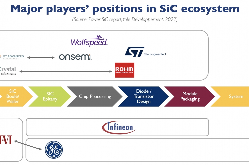
The silicon carbide (SiC) wafer supplier market is experiencing robust growth driven by the accelerating demand for high-performance power electronics, automotive applications, and renewable energy systems. For international B2B buyers from regions such as Africa, South America, the Middle East, and Europe, understanding the evolving market landscape is crucial to securing reliable, cost-effective SiC wafer sources that align with strategic goals.
Global Drivers: The widespread adoption of electric vehicles (EVs), industrial automation, and 5G infrastructure expansion are primary growth catalysts. SiC wafers offer superior thermal conductivity, higher breakdown voltage, and efficiency advantages over traditional silicon wafers, making them indispensable in power semiconductors. This shift is particularly notable in Europe and Australia, where government incentives for clean energy and EV adoption are propelling demand.
Emerging Sourcing Trends:
- Vertical Integration: Leading suppliers are increasingly adopting vertical integration to control quality and reduce lead times, a key consideration for buyers in regions with longer supply chains.
- Customization and Smaller Batch Production: Suppliers are offering more tailored wafer sizes and specifications to accommodate diverse end-use applications, benefiting niche markets in Africa and South America.
- Digital Supply Chain Platforms: Enhanced transparency and real-time tracking through digital procurement platforms are gaining traction, aiding buyers in mitigating supply disruptions and optimizing inventory management.
- Strategic Partnerships: Collaborations between wafer producers and device manufacturers are strengthening, facilitating innovation and reducing time-to-market.
Market Dynamics:
- Supply Constraints: Limited global production capacity and complex manufacturing processes have led to supply bottlenecks, emphasizing the importance of early engagement and long-term contracts.
- Price Volatility: Prices are influenced by raw material availability, geopolitical factors, and technological advancements, necessitating flexible procurement strategies.
- Regional Considerations: Buyers from Africa and the Middle East should account for logistics challenges and customs regulations, while European and South American companies may benefit from proximity to established suppliers and trade agreements.
Sustainability has become a pivotal factor in the procurement of SiC wafers, as buyers worldwide increasingly prioritize environmental impact and ethical sourcing in their supply chains. For B2B buyers, particularly from regions with strong regulatory frameworks like Europe and emerging sustainability mandates in other continents, integrating green principles into sourcing decisions is a competitive advantage.
Environmental Impact: The SiC wafer manufacturing process is energy-intensive, involving high-temperature crystal growth and wafer slicing techniques. Suppliers committed to reducing carbon footprints typically invest in renewable energy-powered production facilities and implement waste reduction protocols. Buyers should inquire about energy consumption metrics and emission reporting to assess supplier sustainability claims.
Ethical Supply Chains: Transparency in sourcing raw materials such as silicon and carbon is essential to avoid association with conflict minerals or exploitative labor practices. Certifications like Responsible Minerals Assurance Process (RMAP) or equivalent regional standards provide assurance of ethical compliance. For B2B buyers, requesting supplier audits and supply chain traceability reports is advisable.
Green Certifications & Materials:
- ISO 14001: Environmental management certification indicating continuous improvement in environmental performance.
- RoHS Compliance: Ensures wafers are free from hazardous substances, aligning with global electronics manufacturing standards.
- Eco-Labeling: Some suppliers are adopting eco-labels that certify reduced environmental impact, helping buyers meet corporate sustainability goals.
Integrating sustainability considerations not only mitigates reputational risks but also aligns procurement with evolving regulatory requirements and end-customer expectations, particularly in environmentally conscious markets like Europe and Australia.
The SiC wafer industry has evolved significantly since its inception in the late 20th century. Initially, SiC crystals were difficult and expensive to produce at scale, limiting their use to niche applications such as high-temperature electronics. Advances in crystal growth techniques, particularly the development of the physical vapor transport (PVT) method, enabled larger, higher-quality wafers to be manufactured.
In the past decade, innovation has accelerated due to rising demand for energy-efficient power devices and the proliferation of EVs. This led to the emergence of multiple global players expanding production capacities and refining wafer quality. For B2B buyers, understanding this evolution highlights the importance of supplier expertise and technology maturity when selecting SiC wafer partners.
Overall, the sector’s trajectory points to increasing availability, improved wafer performance, and a growing emphasis on sustainable manufacturing—factors that buyers must weigh to optimize their sourcing strategies in a competitive global market.
How can I effectively vet SiC wafer suppliers to ensure reliability and quality?
Begin by evaluating the supplier’s industry reputation and years of experience with SiC wafers. Request detailed product datasheets and certifications such as ISO 9001, IATF 16949, or industry-specific quality accreditations. For buyers in Africa, South America, the Middle East, and Europe, verifying compliance with international standards (e.g., RoHS, REACH) is crucial. Conduct factory audits or third-party inspections where possible, and ask for sample wafers to test in your own production environment. Transparent communication and references from other international clients can further validate supplier credibility.
What customization options are typically available when sourcing SiC wafers?
Many suppliers offer customization in wafer diameter, thickness, doping concentration, crystal orientation, and surface finish. Some can also provide epitaxial layers tailored to specific device requirements. When dealing internationally, clarify these specifications upfront to avoid miscommunication. Discuss your technical requirements early and confirm the supplier’s capability to meet them consistently. Customization may impact lead times and minimum order quantities, so factor this into your procurement planning.
What are typical minimum order quantities (MOQs) and lead times for SiC wafers, especially for international buyers?
MOQs vary widely based on wafer size, customization, and supplier scale. For standard SiC wafers, MOQs can start from a few pieces but often increase for custom specifications. Lead times generally range from 6 to 12 weeks, influenced by manufacturing complexity and logistics. International buyers should anticipate additional time for export documentation and customs clearance. Establish clear timelines with your supplier and consider buffer periods to accommodate potential delays in shipping or production.
Which payment terms are common for international purchases of SiC wafers, and how can buyers mitigate risks?
Suppliers typically require upfront payment, a letter of credit (LC), or partial advance with balance on delivery. For new or smaller buyers in emerging markets, negotiating staged payments tied to milestones can reduce financial exposure. Using secure payment platforms and confirming supplier bank details independently helps prevent fraud. Additionally, consider trade credit insurance to protect against non-delivery or insolvency, especially when dealing with suppliers in unfamiliar regions.
What quality assurance (QA) processes and certifications should I expect from reputable SiC wafer suppliers?
Leading suppliers implement rigorous QA protocols including wafer surface inspections, defect density measurement, electrical property testing, and dimensional verification. Certifications like ISO 9001, IATF 16949, and compliance with JEDEC or SEMI standards indicate robust quality management systems. International buyers should request detailed QA reports and traceability documentation for each batch. Regular third-party audits and the supplier’s responsiveness to non-conformance issues are also key indicators of quality commitment.
How can I manage logistics and customs challenges when importing SiC wafers internationally?
SiC wafers require careful packaging to prevent contamination and physical damage during transit. Work with suppliers experienced in international shipping who understand export regulations and hazardous material handling if applicable. Engage freight forwarders familiar with your region’s import procedures to streamline customs clearance. Prepare all necessary documentation, including commercial invoices, certificates of origin, and compliance certificates, to avoid delays. Planning for potential tariffs and import duties is essential for accurate cost forecasting.
What steps should I take if there is a dispute regarding product quality or delivery with my SiC wafer supplier?
First, document all issues thoroughly with photos, test results, and correspondence. Review your purchase agreement’s terms on warranty, returns, and dispute resolution. Engage the supplier promptly to seek amicable resolution through negotiation or mediation. For international disputes, consider involving trade chambers or arbitration bodies such as the ICC. Maintaining clear communication channels and keeping detailed records throughout the transaction will strengthen your position and facilitate faster resolution.
Are there regional considerations when sourcing SiC wafers from suppliers in Asia versus Europe or North America?
Yes, regional differences impact pricing, lead times, and support services. Asian suppliers often offer competitive pricing and larger production volumes but may have longer shipping times and require more attention to quality assurance. European and North American suppliers typically provide closer technical support, faster delivery, and stringent quality controls, albeit at higher costs. International buyers should weigh these factors alongside logistics complexity and after-sales service availability when selecting suppliers to optimize total value.
The information provided in this guide, including content regarding manufacturers, technical specifications, and market analysis, is for informational and educational purposes only. It does not constitute professional procurement advice, financial advice, or legal advice.
While we have made every effort to ensure the accuracy and timeliness of the information, we are not responsible for any errors, omissions, or outdated information. Market conditions, company details, and technical standards are subject to change.
B2B buyers must conduct their own independent and thorough due diligence before making any purchasing decisions. This includes contacting suppliers directly, verifying certifications, requesting samples, and seeking professional consultation. The risk of relying on any information in this guide is borne solely by the reader.
In today’s dynamic semiconductor landscape, sourcing silicon carbide (SiC) wafers demands a strategic approach that balances quality, cost-efficiency, and supply chain resilience. For B2B buyers across Africa, South America, the Middle East, and Europe, understanding the nuances of supplier capabilities, technological advancements, and regional logistics is essential to securing a competitive edge. Prioritizing suppliers with robust R&D, proven quality certifications, and flexible production scales will help mitigate risks associated with global demand fluctuations.
Illustrative Image (Source: Google Search)
Key takeaways include:
Looking forward, the SiC wafer supply chain is poised for innovation and expansion, driven by growing global demand and advancements in fabrication technology. International buyers are encouraged to proactively engage with suppliers who demonstrate agility and sustainability commitments. By embedding strategic sourcing principles into procurement processes today, businesses will not only secure reliable SiC wafer supply but also position themselves to capitalize on emerging opportunities in the electrification and power electronics sectors.
Tags: Black Silicon Carbide, White Fused Alumina, Brown Fused Alumina, Pink Fused Alumina, Black Fused Alumina