In the rapidly evolving landscape of semiconductor technology, international B2B buyers face a critical challenge: sourcing high-quality silicon carbide wafers that meet stringent performance criteria. The demand for silicon carbide (SiC) is surging, driven by its unique properties that enhance efficiency in applications ranging from electric vehicles to renewable energy systems. This guide offers a comprehensive exploration of the global market for silicon carbide wafer manufacturers, equipping buyers with the insights needed to navigate this complex arena effectively.
Within these pages, you will discover an in-depth analysis of various types of silicon carbide wafers, their diverse applications across multiple industries, and essential criteria for vetting potential suppliers. Moreover, we will provide actionable insights on cost considerations and procurement strategies tailored for international buyers, particularly those operating in Africa, South America, the Middle East, and Europe, including key markets like Spain and Indonesia.
By empowering buyers with knowledge and strategic frameworks, this guide aims to facilitate informed purchasing decisions that align with their unique business needs. Whether you are sourcing for a startup or a large enterprise, understanding the nuances of the silicon carbide wafer market is vital for optimizing your supply chain and ensuring competitive advantage in today's technology-driven world.
| Type Name | Key Distinguishing Features | Primary B2B Applications | Brief Pros & Cons for Buyers |
|---|---|---|---|
| Single Crystal Wafer | High purity, excellent electrical properties, uniform thickness | Power electronics, RF devices, LED lighting | Pros: Superior performance; Cons: Higher cost |
| Polycrystalline Wafer | Lower cost, less uniformity, good for large-scale production | Solar cells, industrial applications | Pros: Cost-effective; Cons: Lower efficiency |
| Epitaxial Wafer | Layered structure, customizable properties | Advanced semiconductor devices | Pros: Tailored performance; Cons: Complex fabrication |
| Silicon Carbide-on-Insulator (SiCOI) | Reduced parasitic capacitance, improved thermal performance | High-frequency devices, automotive applications | Pros: Enhanced performance; Cons: Limited availability |
| Thin Wafer Technology | Reduced thickness, lightweight | Mobile devices, compact electronics | Pros: Space-saving; Cons: Fragility during handling |
Single crystal silicon carbide (SiC) wafers are characterized by their high purity and exceptional electrical properties, making them ideal for high-performance applications such as power electronics and RF devices. Their uniform thickness ensures consistent performance across devices. B2B buyers should consider the higher cost associated with these wafers, which is justified by their superior performance and reliability in critical applications.
Polycrystalline SiC wafers are a cost-effective alternative, offering lower prices due to their less stringent production processes. While they provide adequate performance for applications like solar cells and industrial uses, they lack the uniformity and efficiency of single crystal wafers. B2B buyers should weigh the benefits of reduced costs against the potential for lower efficiency in their applications.
Epitaxial wafers feature a layered structure that allows for customizable electrical properties tailored to specific applications. This makes them especially valuable in advanced semiconductor devices. However, the complexity of their fabrication can lead to higher prices. B2B buyers looking for specialized performance should consider the advantages of epitaxial wafers, despite the associated costs.
SiCOI wafers are designed to reduce parasitic capacitance and improve thermal performance, making them suitable for high-frequency devices and automotive applications. These wafers provide enhanced performance compared to traditional SiC wafers, but their limited availability can pose a challenge for buyers. It’s essential for B2B buyers to evaluate their specific needs against the potential supply constraints.
Thin wafer technology provides a lightweight solution that is particularly advantageous for mobile devices and compact electronics. While their reduced thickness allows for significant space savings, these wafers can be fragile, necessitating careful handling during production and integration. B2B buyers should consider the trade-off between space efficiency and handling challenges when opting for thin wafers.
Related Video: Silicon Wafer Manufacturers | What is Gettering and its Importance in Wafer Manufacturing
| Industry/Sector | Specific Application of Silicon Carbide Wafer Manufacturers | Value/Benefit for the Business | Key Sourcing Considerations for this Application |
|---|---|---|---|
| Semiconductor Industry | Power Electronics in Electric Vehicles (EVs) | Enhanced efficiency and thermal management in EV systems | Ensure compliance with international standards and quality certifications. |
| Telecommunications | RF Devices and 5G Infrastructure | Improved signal integrity and reduced energy consumption | Evaluate the supplier's technological capabilities and reliability. |
| Renewable Energy | Solar Inverters | Increased efficiency in energy conversion and lower costs | Focus on suppliers who can provide long-term warranties and support. |
| Aerospace & Defense | High-Temperature Sensors | Improved durability and performance under extreme conditions | Assess the supplier's experience with aerospace-grade materials. |
| Industrial Automation | Motor Drives and Control Systems | Higher performance and reliability in automation applications | Verify the supplier's ability to meet specific industry requirements and certifications. |
In the semiconductor industry, silicon carbide (SiC) wafers are crucial for manufacturing power electronics used in electric vehicles (EVs). These wafers enable devices to operate at higher voltages and temperatures, enhancing efficiency and thermal management. For international buyers, particularly those in regions like Africa and South America, it is essential to partner with manufacturers that comply with international quality standards to ensure performance reliability in automotive applications.
Silicon carbide wafers play a significant role in the telecommunications sector, particularly in the production of RF devices and 5G infrastructure. The use of SiC enhances signal integrity and reduces energy consumption, which is vital for the growing demand for faster and more reliable communication networks. Buyers should prioritize suppliers with advanced technological capabilities to ensure they can meet the rigorous demands of modern telecommunication systems.
In renewable energy, silicon carbide wafers are integral to manufacturing solar inverters, which convert solar energy into usable electricity. These wafers increase efficiency in energy conversion, ultimately lowering costs for end-users. For B2B buyers in Europe and the Middle East, sourcing from manufacturers that provide long-term warranties and technical support can significantly enhance project viability and reduce operational risks.
Silicon carbide wafers are utilized in high-temperature sensors within the aerospace and defense industries. These sensors are designed to withstand extreme conditions, improving durability and performance. Buyers in these sectors should assess a supplier's experience with aerospace-grade materials to ensure compliance with stringent safety and performance standards.
In industrial automation, silicon carbide wafers are essential for motor drives and control systems. They provide higher performance and reliability, critical for the efficient operation of automated systems. For international buyers, it is important to verify a supplier's ability to meet specific industry certifications and requirements to ensure compatibility with existing systems and processes.
Related Video: Polishing Processes Behind Silicon Wafer Production | Wafer World
The Problem:
International B2B buyers often struggle to find reliable suppliers of high-quality silicon carbide wafers that meet their specific technical and quality standards. This challenge is especially pronounced for companies in Africa and South America, where local suppliers may not be equipped with the necessary technology or standards. The risk of receiving subpar products can lead to increased operational costs and project delays, significantly impacting the supply chain and overall business performance.
The Solution:
To overcome this sourcing challenge, buyers should prioritize working with manufacturers that have established quality certifications, such as ISO 9001 or IATF 16949. Conduct thorough due diligence by requesting product samples and conducting on-site visits if possible. Leverage platforms like Alibaba or ThomasNet to compare manufacturers based on customer reviews and ratings. It is also beneficial to engage with regional trade shows and industry expos, where buyers can meet manufacturers face-to-face and assess their capabilities directly. Establishing a long-term relationship with a reputable supplier can ensure a consistent supply of high-quality wafers.
The Problem:
Many B2B buyers encounter confusion when trying to navigate the complex technical specifications of silicon carbide wafers, such as thickness, diameter, and substrate type. This can lead to incorrect orders or mismatched expectations, which may compromise the performance of their applications, particularly in high-power electronics or automotive sectors. This challenge is amplified for buyers from regions with less access to technical resources and expertise.
The Solution:
To effectively address these technical challenges, buyers should invest in training their procurement and engineering teams on the essential specifications of silicon carbide wafers. Collaborating with suppliers who provide technical support or consultation services can also bridge the knowledge gap. Additionally, engaging in forums or online communities focused on semiconductor manufacturing can help buyers gain insights into best practices and common pitfalls. Buyers should also prepare a detailed specifications document outlining their needs before approaching manufacturers, ensuring clarity and reducing the likelihood of errors in orders.
The Problem:
Long lead times and delivery uncertainties pose significant issues for B2B buyers in the silicon carbide wafer market. Many manufacturers operate on just-in-time production schedules, which can lead to delays in fulfilling orders. This is particularly problematic for buyers in the Middle East and Europe, where timely product availability is critical for maintaining competitive advantages in fast-paced industries like renewable energy and telecommunications.
The Solution:
To mitigate lead time issues, buyers should establish clear communication channels with their suppliers regarding expected timelines and potential risks. It is advisable to implement a robust inventory management system that accounts for lead time variability, allowing for better planning and buffer stock management. Additionally, forming strategic partnerships with multiple suppliers can provide flexibility and alternative sourcing options in case of delays. Buyers should also discuss expedited shipping options or local warehousing arrangements with manufacturers to ensure timely delivery. Regular performance reviews with suppliers can help address any recurring issues and foster a proactive relationship focused on continuous improvement.
Silicon carbide (SiC) wafers are critical components in various high-performance applications, particularly in the semiconductor industry. Selecting the right materials for wafer manufacturing is essential to ensure optimal performance, durability, and cost-effectiveness. Below, we analyze some of the most common materials used in silicon carbide wafer manufacturing.
Silicon Carbide (SiC)
- Key Properties: SiC is known for its high thermal conductivity, exceptional hardness, and resistance to thermal shock. It can withstand high temperatures (up to 1600°C) and has a high breakdown voltage, making it suitable for high-power applications.
- Pros & Cons: The advantages of SiC include its ability to operate at higher temperatures and voltages compared to traditional silicon wafers, which enhances efficiency in power electronics. However, the manufacturing process can be complex and costly, which may deter some manufacturers.
- Impact on Application: SiC wafers are particularly effective in high-frequency and high-temperature applications, such as electric vehicles and renewable energy systems. Their compatibility with harsh environments makes them a preferred choice in aerospace and defense sectors.
- Considerations for International Buyers: Buyers from Africa, South America, the Middle East, and Europe should consider compliance with international standards such as ASTM and JIS. The availability of SiC materials can vary by region, impacting supply chain logistics.
Gallium Nitride (GaN)
- Key Properties: GaN has excellent thermal conductivity and a wide bandgap, which allows it to function efficiently at high voltages and temperatures.
- Pros & Cons: GaN wafers are highly efficient for RF applications and offer high electron mobility. However, they can be more expensive than SiC and may require specialized manufacturing processes.
- Impact on Application: GaN is widely used in RF and microwave applications, making it ideal for telecommunications and satellite communications.
- Considerations for International Buyers: Compliance with regional standards is crucial, particularly for telecommunications applications. Buyers should also assess the availability of GaN substrates in their local markets.
Aluminum Nitride (AlN)
- Key Properties: AlN features high thermal conductivity and excellent electrical insulation properties. It can operate at high temperatures and has a high breakdown voltage.
- Pros & Cons: AlN is advantageous for applications requiring good thermal management, such as high-power devices. However, its brittleness can pose challenges during processing and handling.
- Impact on Application: AlN wafers are suitable for high-frequency applications and are often used in LED technology and power electronics.
- Considerations for International Buyers: Buyers should be aware of the specific thermal and electrical requirements of their applications, as well as the availability of AlN substrates that meet international standards.
Silicon (Si)
- Key Properties: Silicon is the most widely used semiconductor material due to its abundance and well-understood properties. It has moderate thermal conductivity and is cost-effective.
- Pros & Cons: Silicon wafers are less expensive and easier to manufacture than SiC or GaN. However, they have lower thermal and electrical performance, which may limit their use in high-power applications.
- Impact on Application: Silicon is suitable for a wide range of electronic applications, including consumer electronics and integrated circuits.
- Considerations for International Buyers: Buyers should consider the cost-effectiveness of silicon wafers for their applications, as well as compliance with local regulations and standards.
| Material | Typical Use Case for silicon carbide wafer manufacturers | Key Advantage | Key Disadvantage/Limitation | Relative Cost (Low/Med/High) |
|---|---|---|---|---|
| Silicon Carbide (SiC) | High-frequency, high-temperature applications | High thermal conductivity and breakdown voltage | Complex and costly manufacturing | High |
| Gallium Nitride (GaN) | RF and microwave applications | High efficiency for RF applications | Higher cost and specialized manufacturing | High |
| Aluminum Nitride (AlN) | High-frequency and LED technology | Excellent thermal management | Brittle and challenging to process | Medium |
| Silicon (Si) | Consumer electronics and integrated circuits | Cost-effective and widely available | Lower thermal and electrical performance | Low |
This strategic material selection guide provides international B2B buyers with critical insights into the materials used in silicon carbide wafer manufacturing, enabling informed decision-making based on performance, cost, and application suitability.
The manufacturing of silicon carbide (SiC) wafers involves several critical stages, each designed to ensure the highest quality and performance standards. Understanding these stages is essential for B2B buyers looking to procure reliable products from manufacturers.
The first step in the SiC wafer manufacturing process is the preparation of raw materials. High-purity silicon and carbon sources are combined at high temperatures in a chemical vapor deposition (CVD) process. This process results in the formation of silicon carbide crystals. Buyers should look for suppliers who utilize high-quality raw materials, as the purity of the input materials directly affects the final product's performance and reliability.
After preparing the raw materials, the next stage is the growth of silicon carbide crystals. This is typically achieved through methods such as the physical vapor transport (PVT) or the sublimation method. During this process, the temperature and pressure must be meticulously controlled to ensure the desired crystal structure and size. For international buyers, it is crucial to inquire about the specific crystal growth methods employed by potential suppliers, as this can influence the material's electrical and thermal properties.
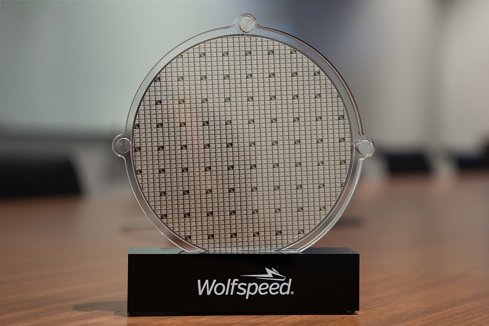
A stock image related to silicon carbide wafer manufacturers.
Once the SiC crystals are grown, they are sliced into wafers using diamond saws or wire saws. This step requires precision to ensure that the wafers are of uniform thickness and size, typically ranging from 2 to 6 inches in diameter. The slicing process also generates kerf loss, which buyers should consider when evaluating the cost-effectiveness of a supplier's products.
Following wafer slicing, the wafers undergo a series of surface finishing processes. This includes grinding, polishing, and cleaning to achieve a smooth surface finish. The surface quality is paramount for applications in electronics and power devices, as any imperfections can lead to device failures. B2B buyers should request information about the surface treatment processes used by manufacturers to ensure they meet their specific application requirements.
Quality assurance is a critical aspect of silicon carbide wafer manufacturing. International standards and industry-specific certifications guide manufacturers in maintaining high-quality production processes.
Manufacturers of silicon carbide wafers often adhere to international quality management standards such as ISO 9001. This certification demonstrates a commitment to continuous improvement and customer satisfaction. Additionally, industry-specific standards such as CE marking for compliance with European safety and environmental regulations or API specifications for the oil and gas sector may also apply. B2B buyers should verify these certifications during the supplier evaluation process.
Quality control is integrated throughout the manufacturing process, with various checkpoints to ensure product integrity:
Incoming Quality Control (IQC): This initial checkpoint assesses the quality of raw materials before they enter the production process. Suppliers should provide documentation demonstrating that their materials meet specified quality standards.
In-Process Quality Control (IPQC): During manufacturing, continuous monitoring of processes ensures that any deviations from set parameters are promptly addressed. This might include real-time testing of temperature and pressure during crystal growth.
Final Quality Control (FQC): Once the wafers are completed, they undergo rigorous testing to confirm that they meet specified electrical and physical properties. Common tests include electrical conductivity tests, surface roughness measurements, and visual inspections for defects.
Testing methods are essential for verifying the quality of silicon carbide wafers. B2B buyers should be familiar with these methods to assess the reliability of their suppliers.
Electrical Testing: This includes measuring the resistivity and breakdown voltage of the wafers, which are critical parameters for semiconductor applications. Advanced techniques such as Hall effect measurements can provide insights into the material's carrier concentration and mobility.
Microscopic Inspection: Scanning electron microscopy (SEM) and atomic force microscopy (AFM) are commonly used to analyze surface morphology and identify defects at the microscopic level. Buyers should request reports detailing these inspections to ensure the wafers meet their specifications.
Thermal Testing: Given that silicon carbide is often used in high-temperature applications, thermal conductivity tests are essential. These tests ensure that the wafers can perform under operational conditions without degradation.
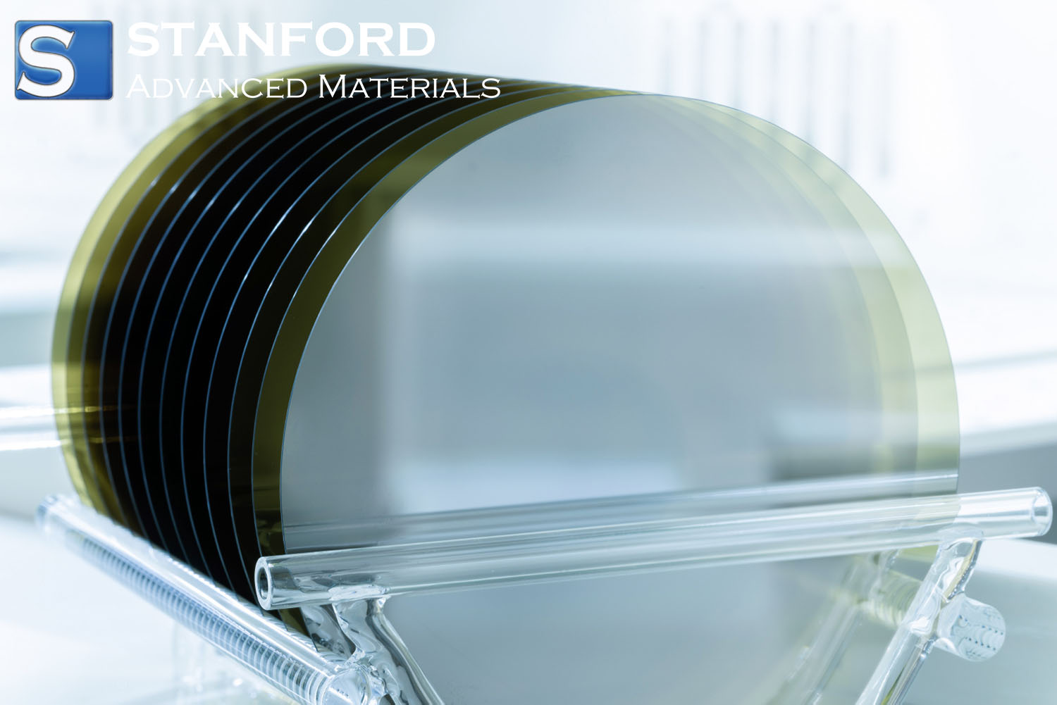
A stock image related to silicon carbide wafer manufacturers.
For international B2B buyers, verifying the quality control processes of silicon carbide wafer manufacturers is critical to ensuring product reliability. Here are actionable steps to consider:
Request to conduct on-site audits of potential suppliers. This allows buyers to observe manufacturing processes, quality control measures, and compliance with international standards firsthand. Audits should include an evaluation of equipment, cleanliness, and adherence to safety protocols.
Ask suppliers for comprehensive quality reports that detail their testing methods and results. These reports should include data on IQC, IPQC, and FQC checkpoints, as well as any non-conformance issues encountered during production and the corrective actions taken.
Consider engaging third-party inspection services to evaluate the quality of products before shipment. Independent inspections can provide additional assurance regarding the integrity of the wafers and compliance with specified standards.
Understanding the nuances of quality certifications is vital for B2B buyers from diverse regions, including Africa, South America, the Middle East, and Europe. Here are key considerations:
Regional Compliance: Different regions may have varying compliance requirements. For instance, European buyers must ensure that products comply with CE marking, while buyers in the Middle East may require adherence to specific local standards.
Documentation Requirements: Ensure that suppliers provide all necessary documentation, including material safety data sheets (MSDS), compliance certificates, and test reports. This documentation is essential for customs clearance and regulatory compliance.
Language and Communication: Language barriers can pose challenges during quality verification. Buyers should ensure that suppliers can provide documentation in a language they understand, or arrange for translation services if necessary.
By focusing on these aspects of manufacturing processes and quality assurance, B2B buyers can make informed decisions when sourcing silicon carbide wafers, ensuring they partner with reliable manufacturers who meet their specific needs.
Sourcing silicon carbide wafers is a critical step for businesses looking to leverage the unique properties of this semiconductor material. Silicon carbide (SiC) is increasingly favored in various applications, including power electronics and high-temperature environments. This checklist serves as a practical guide to help B2B buyers—particularly from Africa, South America, the Middle East, and Europe—navigate the procurement process effectively.
Clarifying your technical requirements is the first step in sourcing silicon carbide wafers. Consider factors such as wafer size, thickness, and crystal orientation, as these specifications will directly impact the performance of your end product.
Conduct thorough market research to identify potential suppliers of silicon carbide wafers. Look for manufacturers with a proven track record in the industry and expertise in silicon carbide technology.
Before committing, it's crucial to vet suppliers thoroughly. Assess their production capabilities, including equipment, technology, and quality control processes.
Ensure that your potential suppliers hold relevant certifications that validate their quality management and environmental practices. Certifications such as ISO 9001 for quality management or ISO 14001 for environmental management are essential indicators of a reputable supplier.
Before finalizing your supplier, request samples of their silicon carbide wafers for testing. This step allows you to evaluate the material's performance against your specifications.
Once you've evaluated potential suppliers, it's time to negotiate terms and conditions. Discuss pricing, lead times, payment terms, and warranty policies to ensure a mutually beneficial agreement.
Effective communication is vital for a successful sourcing relationship. Establish a clear plan for ongoing communication with your supplier to address any issues that may arise during production or delivery.
By following this step-by-step checklist, international B2B buyers can streamline their sourcing process for silicon carbide wafers, ensuring that they partner with reliable suppliers who meet their technical and operational needs.
Understanding the cost structure of silicon carbide (SiC) wafer manufacturing is crucial for international B2B buyers. The primary cost components include:
Materials: Silicon carbide itself is a high-cost raw material, influenced by purity and sourcing. The quality of SiC impacts the performance of the wafers, making it essential to consider suppliers who offer high-grade materials.
Labor: Skilled labor is necessary for handling the sophisticated manufacturing processes, which can drive up costs. Labor costs vary significantly across regions, impacting overall pricing.
Manufacturing Overhead: This includes costs related to facility maintenance, utilities, and equipment depreciation. High-tech manufacturing environments require significant investment in infrastructure, which contributes to the overhead costs.
Tooling: Custom tooling for wafer production is another substantial cost. The initial investment in specialized tools can be high, but they are necessary for precision manufacturing.
Quality Control (QC): Rigorous QC processes are essential to ensure that wafers meet industry standards. The costs associated with testing and certification can add significantly to the overall expenses.
Logistics: Shipping and handling costs can vary based on the location of both the manufacturer and the buyer. Consideration of local tariffs, shipping routes, and lead times is critical for budgeting.
Margin: Finally, the profit margin that manufacturers add to the base cost can vary. It is influenced by market conditions and competition, impacting the final pricing for buyers.
Several factors can influence the pricing of silicon carbide wafers, making it important for buyers to understand these nuances:
Volume and Minimum Order Quantity (MOQ): Larger orders typically reduce per-unit costs. Buyers should negotiate terms that allow for bulk purchasing to achieve better pricing.
Specifications and Customization: Customized wafers tailored to specific applications can command higher prices. Buyers must weigh the benefits of customization against the additional costs.
Materials and Quality Certifications: The grade of silicon carbide and relevant certifications (like ISO or RoHS compliance) can affect pricing. Higher-quality materials may have a premium, but they can provide better performance and longevity.
Supplier Factors: The reliability, reputation, and location of the supplier play a significant role in pricing. Established suppliers with a track record may charge more but often provide better service and quality assurance.
Incoterms: Understanding the Incoterms (International Commercial Terms) can help buyers manage shipping costs and responsibilities. Different terms can affect the total landed cost of the product.
For international B2B buyers, especially from Africa, South America, the Middle East, and Europe, the following strategies can help optimize sourcing:
Negotiate Smartly: Engage in discussions to understand the supplier's pricing structure. Leverage long-term relationships or potential future orders to negotiate better terms.
Focus on Cost-Efficiency: Consider not just the purchase price but the Total Cost of Ownership (TCO). This includes operational costs, maintenance, and potential downtime due to wafer failure.
Understand Pricing Nuances: Familiarize yourself with regional market trends. Prices can fluctuate based on demand, regional supply chain issues, and geopolitical factors.
Evaluate Multiple Suppliers: Don’t settle for the first quote. Compare offerings from multiple suppliers to ensure you’re getting competitive pricing and quality.
Request Transparent Pricing: Ask suppliers for a breakdown of costs to identify areas where you might negotiate or seek alternative solutions.
The prices for silicon carbide wafers can vary widely based on the factors discussed above. This analysis provides indicative cost structures and pricing influences but should not be considered fixed. It is advisable for buyers to conduct thorough market research and engage in direct discussions with suppliers for accurate and up-to-date pricing information.
In the rapidly evolving semiconductor industry, B2B buyers must assess various options when considering silicon carbide (SiC) wafers. While silicon carbide wafers are renowned for their high thermal conductivity and efficiency in power electronics, alternative solutions can also fulfill similar requirements. This section provides a comparative analysis of silicon carbide wafer manufacturers against two viable alternatives: Gallium Nitride (GaN) wafers and traditional silicon wafers.
| Comparison Aspect | Silicon Carbide Wafer Manufacturers | Gallium Nitride Wafer Manufacturers | Traditional Silicon Wafer Manufacturers |
|---|---|---|---|
| Performance | High efficiency, excellent thermal conductivity, suitable for high-voltage applications | Superior efficiency for RF applications, low power loss | Adequate for standard applications, lower efficiency in high-power contexts |
| Cost | Higher initial investment | Moderate to high cost | Generally lower cost |
| Ease of Implementation | Complex integration in existing systems | Requires specialized handling | Widely compatible, easier integration |
| Maintenance | Requires less frequent replacement | Similar durability as SiC | More frequent replacements needed |
| Best Use Case | Electric vehicles, industrial power supplies | RF amplifiers, LED technology | Consumer electronics, general-purpose applications |
Gallium Nitride (GaN) wafers are a prominent alternative to silicon carbide wafers, especially in applications requiring high-frequency and high-power electronics. GaN is celebrated for its remarkable efficiency in converting power, making it ideal for RF amplifiers and LED technologies.
Pros: GaN wafers exhibit lower power losses and can operate at higher voltages than traditional silicon, which can lead to smaller and lighter devices. They are also becoming more cost-competitive as production technologies improve.
Cons: However, GaN wafers require specialized handling and integration processes, which may pose challenges for manufacturers already accustomed to silicon-based technologies. The initial investment can also be a barrier for some businesses.
Traditional silicon wafers have been the backbone of the semiconductor industry for decades. They are widely used in consumer electronics and general-purpose applications due to their lower cost and ease of integration.
Pros: The compatibility of silicon wafers with existing manufacturing processes makes them an accessible option for many businesses. Additionally, the extensive knowledge base and supply chain for silicon technology facilitate smoother operations.
Cons: On the downside, silicon wafers often fall short in high-performance applications, particularly in terms of thermal efficiency and power handling when compared to silicon carbide and gallium nitride alternatives. This can lead to larger, less efficient designs in power electronics.
When selecting a semiconductor solution, B2B buyers should conduct a thorough analysis of their specific needs. Considerations such as performance requirements, budget constraints, and existing manufacturing capabilities are crucial. For high-performance applications like electric vehicles or power supplies, silicon carbide wafers may be the best fit despite their higher cost. Conversely, for applications in consumer electronics or where budget constraints are significant, traditional silicon wafers could suffice.
Ultimately, aligning the choice of materials and technologies with the specific demands of the application will lead to optimized performance and cost-effectiveness. Engaging with manufacturers and conducting pilot tests can also provide valuable insights into the most suitable alternative for your business needs.
When sourcing silicon carbide (SiC) wafers, understanding the technical specifications is vital for ensuring compatibility with your production processes. Here are critical properties that B2B buyers should consider:
Material grade refers to the purity and quality of silicon carbide used in wafer production. High-grade SiC wafers exhibit superior electrical and thermal conductivity, making them essential for high-performance applications such as power electronics and high-frequency devices. For buyers, selecting the appropriate grade can significantly impact the performance and reliability of the final product.
Tolerance indicates the allowable deviation from specified dimensions during the manufacturing process. In silicon carbide wafers, tight tolerances are crucial, especially in applications requiring precise alignment and minimal defects. Understanding tolerance specifications helps buyers ensure that the wafers meet their exact needs, reducing the risk of production downtime or costly reworks.
The thickness of silicon carbide wafers is critical as it affects the mechanical strength and thermal conductivity of the materials. Thicker wafers may provide better durability but can also increase costs and weight. Buyers should evaluate the thickness based on their specific applications, such as LED manufacturing or semiconductor devices, to ensure optimal performance.
Silicon carbide wafers come in various diameters, commonly ranging from 2 inches to 6 inches and beyond. The diameter impacts the number of chips that can be fabricated from a single wafer, thus influencing production efficiency and cost-effectiveness. Buyers must consider their production scale and chip size requirements when selecting wafer diameters.
Surface quality is a measure of the smoothness and defect density on the wafer's surface. High-quality surfaces are essential for applications that require precise electronic properties and minimal scattering of light, such as in photonics and high-voltage devices. Buyers should prioritize surface quality specifications to ensure optimal performance in their applications.
Navigating the silicon carbide wafer market also requires familiarity with industry jargon. Here are some common terms that buyers should understand:
An OEM refers to a company that produces components or equipment that are then sold under another brand’s name. In the context of silicon carbide wafers, buyers may work with OEMs to incorporate these materials into their products, often requiring specific technical specifications and quality standards.
MOQ is the smallest quantity of a product that a supplier is willing to sell. Understanding the MOQ is crucial for buyers, particularly those who may not need large quantities of silicon carbide wafers but still require consistent supply and quality.
An RFQ is a formal document sent to suppliers requesting pricing and terms for specific products. B2B buyers should prepare detailed RFQs that include specifications like material grade, tolerance, and quantity to receive accurate quotes from manufacturers.
Incoterms define the responsibilities of buyers and sellers regarding shipping, insurance, and tariffs. Familiarity with these terms helps buyers understand their obligations and manage costs effectively when importing silicon carbide wafers from international suppliers.
Lead time refers to the time taken from placing an order to receiving the goods. This is a critical factor for B2B buyers who need to plan their production schedules. Understanding lead times allows for better inventory management and project planning.
By grasping these essential technical properties and trade terms, international B2B buyers can make informed decisions that enhance their sourcing strategies for silicon carbide wafers.
The silicon carbide (SiC) wafer market is witnessing significant growth driven by the increasing demand for high-performance semiconductors across various industries. The global shift towards electric vehicles (EVs), renewable energy sources, and advanced electronics has positioned SiC wafers as a crucial component due to their superior thermal conductivity and efficiency compared to traditional silicon wafers. In regions like Africa and South America, where there is a burgeoning interest in clean technology, the adoption of SiC technology is expected to rise sharply, aligning with international sustainability goals.
Emerging B2B technology trends, such as the integration of artificial intelligence in manufacturing processes and advancements in wafer fabrication techniques, are enhancing the scalability and efficiency of SiC production. Moreover, international buyers are increasingly seeking suppliers who can offer not only competitive pricing but also innovative solutions that align with their specific operational requirements. The market dynamics indicate a shift towards strategic partnerships and collaborations, enabling manufacturers to optimize supply chains and reduce lead times.
Sustainability is becoming a cornerstone of procurement strategies for international B2B buyers, particularly in the silicon carbide wafer sector. The environmental impact of mining and processing raw materials for SiC production cannot be overlooked. As a result, buyers must prioritize suppliers who adhere to ethical sourcing practices, ensuring that their materials are obtained responsibly and with minimal ecological disruption.
Buyers can look for suppliers with 'green' certifications, such as ISO 14001, which indicates a commitment to environmental management. Additionally, utilizing recycled materials in the production of silicon carbide wafers can significantly mitigate environmental impact. Understanding the supply chain is crucial; buyers should seek transparency regarding sourcing practices and the carbon footprint associated with production. By engaging with manufacturers who prioritize sustainability, B2B buyers not only contribute to environmental preservation but also enhance their brand reputation in an increasingly eco-conscious market.
Silicon carbide was first synthesized in 1891, but its industrial applications gained traction in the late 20th century as the demand for high-performance materials surged. Initially used for abrasives and cutting tools, SiC's semiconductor properties began to be recognized in the 1970s, paving the way for its use in electronics. The evolution of silicon carbide wafers has been marked by significant technological advancements, leading to improved purity and crystal structure, which are critical for semiconductor applications.
As industries moved towards miniaturization and energy efficiency, the demand for SiC wafers exploded, particularly in the automotive and power electronics sectors. Today, the historical development of silicon carbide wafers is not only a testament to material science innovation but also reflects the growing importance of sustainable practices in manufacturing processes, making it a pivotal choice for B2B buyers globally.
How do I choose the right silicon carbide wafer manufacturer for my needs?
Selecting the right manufacturer involves assessing several factors. Start by examining their production capacity and quality control processes. Request samples to evaluate the wafer's electrical and thermal properties. Look for certifications like ISO 9001, which indicates adherence to quality management standards. Additionally, consider their experience in your specific industry sector and their ability to customize products according to your requirements. Finally, check references or reviews from other clients to gauge reliability and customer service.
What are the typical applications for silicon carbide wafers in various industries?
Silicon carbide wafers are widely used in power electronics, including devices like MOSFETs and Schottky diodes, due to their high thermal conductivity and efficiency. They are also integral in automotive applications, particularly in electric vehicles for power management systems. In telecommunications, they support high-frequency applications. Additionally, silicon carbide is crucial in manufacturing high-performance LEDs and laser diodes, making it valuable across sectors from consumer electronics to industrial automation.
What customization options are available when sourcing silicon carbide wafers?
Many manufacturers offer customization to meet specific application requirements. Customization can include variations in wafer size, thickness, and doping levels. Buyers can also specify surface finishes, such as polished or epitaxial layers, to enhance performance. It's essential to communicate your precise needs early in the sourcing process, as this will help manufacturers provide the most suitable solutions. Ensure that you confirm their capability to meet your customization requests without compromising on quality or delivery timelines.
What is the minimum order quantity (MOQ) for silicon carbide wafers?
The MOQ can vary significantly among manufacturers, typically ranging from a few wafers to several hundred, depending on the production capabilities and the specific type of wafer. Smaller manufacturers might accommodate lower MOQs, while larger companies often have higher thresholds. It’s advisable to discuss your requirements directly with potential suppliers to negotiate favorable terms, especially if you are testing a new application or entering a new market.
What payment terms should I expect when dealing with silicon carbide wafer manufacturers?
Payment terms can vary widely based on the manufacturer and your negotiating power. Common terms include upfront deposits of 30-50%, with the balance due upon delivery or after a specified period. Some suppliers may offer credit terms for established buyers. It's crucial to clarify these terms in advance and ensure they align with your cash flow management. Additionally, consider the implications of currency fluctuations if dealing with international suppliers.
How can I ensure quality assurance when sourcing silicon carbide wafers?
To ensure quality, request detailed documentation regarding the manufacturer's quality assurance protocols. Look for certifications such as ISO 9001 or specific industry-related certifications. Ask for test reports that validate the performance specifications of the wafers. Regular audits of the supplier's production processes and quality control measures can also be beneficial. Establishing a clear agreement on quality standards and expectations before placing an order is critical to maintaining product integrity.
What logistics considerations should I keep in mind when importing silicon carbide wafers?
Logistics are crucial when importing silicon carbide wafers, as they can be sensitive to environmental conditions. Ensure that the supplier uses appropriate packaging to protect the wafers during transit. Understand the shipping methods available, including air freight for faster delivery or sea freight for cost savings. Be aware of customs regulations in your country to avoid delays. Finally, consider working with a freight forwarder experienced in handling electronic components to streamline the process.
How do I vet potential silicon carbide wafer suppliers effectively?
Vetting suppliers involves a comprehensive assessment of their credentials and capabilities. Start by checking their industry experience and technological expertise. Request case studies or references from previous clients to evaluate their performance and reliability. Additionally, visit their manufacturing facilities if possible or conduct virtual audits. Look for suppliers who are transparent about their processes and willing to engage in open communication. Finally, assess their financial stability to ensure they can meet your long-term needs.
The information provided in this guide, including content regarding manufacturers, technical specifications, and market analysis, is for informational and educational purposes only. It does not constitute professional procurement advice, financial advice, or legal advice.
While we have made every effort to ensure the accuracy and timeliness of the information, we are not responsible for any errors, omissions, or outdated information. Market conditions, company details, and technical standards are subject to change.
B2B buyers must conduct their own independent and thorough due diligence before making any purchasing decisions. This includes contacting suppliers directly, verifying certifications, requesting samples, and seeking professional consultation. The risk of relying on any information in this guide is borne solely by the reader.
In the rapidly evolving landscape of silicon carbide wafer manufacturing, strategic sourcing emerges as a critical component for international B2B buyers. By leveraging a well-defined sourcing strategy, businesses can not only enhance their supply chain resilience but also secure competitive pricing and superior product quality. Understanding the unique characteristics of silicon carbide—its high thermal conductivity and electrical properties—enables buyers to make informed decisions that align with their technological needs.
International buyers, particularly from regions like Africa, South America, the Middle East, and Europe, must prioritize partnerships with reputable manufacturers that adhere to stringent quality standards. These partnerships foster innovation, reduce lead times, and ultimately contribute to the sustainability of supply chains. Additionally, engaging with local suppliers can mitigate logistical challenges and foster regional economic growth.
Looking ahead, the demand for silicon carbide in applications such as electric vehicles, renewable energy, and advanced electronics is expected to surge. Buyers should remain vigilant and proactive in their sourcing strategies, exploring new manufacturers and technologies that can meet the evolving market demands. As you navigate this dynamic landscape, consider reaching out to suppliers that not only offer quality products but also share a vision for innovation and sustainability. Your strategic sourcing decisions today will shape the success of your operations tomorrow.
Tags: Black Silicon Carbide, White Fused Alumina, Brown Fused Alumina, Pink Fused Alumina, Black Fused Alumina