Navigating the global market for silicon carbide wafers poses significant challenges for international B2B buyers, particularly those sourcing for industries in Africa, South America, the Middle East, and Europe, including Spain and the UAE. The unique properties of silicon carbide make it a preferred material in high-performance applications, from power electronics to electric vehicles. However, the complexity of sourcing these materials—considering factors like quality assurance, supplier reliability, and cost-effectiveness—can be daunting.
This comprehensive guide addresses these challenges by delving into various types of silicon carbide wafers, their applications across different sectors, and critical insights into supplier vetting processes. We explore the intricacies of pricing, enabling buyers to understand cost dynamics and negotiate better deals. Additionally, this guide provides actionable strategies to ensure compliance with international standards and regulations, which is crucial for businesses operating in diverse markets.
By arming international B2B buyers with the knowledge and tools necessary for effective decision-making, this guide empowers them to navigate the silicon carbide wafer market confidently. Buyers will gain insights into making informed purchasing decisions that align with their operational needs and strategic goals, ultimately enhancing their competitive edge in the global marketplace.
| Type Name | Key Distinguishing Features | Primary B2B Applications | Brief Pros & Cons for Buyers |
|---|---|---|---|
| 4H-SiC Wafers | High thermal conductivity, excellent for high-power applications | Power electronics, RF devices | Pros: High performance in extreme conditions. Cons: Higher cost compared to other types. |
| 6H-SiC Wafers | Good balance of properties, lower defect density | Automotive electronics, LED technology | Pros: Versatile applications. Cons: Moderate thermal conductivity compared to 4H-SiC. |
| Semi-Insulating SiC Wafers | Reduced conductivity, ideal for high-frequency devices | RF and microwave applications | Pros: Minimizes parasitic capacitance. Cons: Limited availability. |
| Epitaxial SiC Wafers | Thin layer of SiC grown on a substrate for enhanced properties | Advanced power devices, high-frequency transistors | Pros: Improved device performance. Cons: More complex manufacturing process. |
| SiC Substrates | Basic form used for various applications, can be further processed | General electronics, research applications | Pros: Cost-effective for bulk applications. Cons: Requires further processing for high-end applications. |
4H-SiC wafers are recognized for their superior thermal conductivity and ability to operate efficiently in high-voltage and high-temperature environments. This makes them ideal for power electronics and radio frequency (RF) devices, particularly in sectors such as renewable energy and electric vehicles. When considering procurement, buyers should evaluate factors such as supplier reliability, wafer uniformity, and the specific thermal requirements of their applications.
6H-SiC wafers offer a balanced combination of electrical and thermal properties, making them suitable for a range of applications from automotive electronics to LED technology. They possess a lower defect density than 4H-SiC, which can enhance device reliability. Buyers should assess their specific application needs, as well as the trade-offs between cost and performance when choosing between 4H and 6H variants.
Semi-insulating SiC wafers are designed to minimize electrical conductivity, making them particularly valuable in RF and microwave applications. Their reduced parasitic capacitance leads to improved performance in high-frequency devices. However, buyers may face challenges in sourcing these wafers due to limited availability, and should consider vendor capabilities in providing consistent quality.
Epitaxial SiC wafers feature a thin layer of silicon carbide that is grown on a substrate, which enhances the electrical properties of the final device. They are particularly beneficial for advanced power devices and high-frequency transistors, where performance is critical. Buyers must consider the complexity of the manufacturing process and the associated costs, as these wafers are typically more expensive than standard wafers.
SiC substrates serve as the foundational material for various electronic applications and can be processed further to meet specific needs. They are cost-effective for bulk applications and are widely used in research settings. However, buyers should be aware that while substrates are versatile, they may require additional processing to achieve high-performance standards in advanced applications.
Related Video: What Are Silicon Carbide Wafers? - Chemistry For Everyone
| Industry/Sector | Specific Application of Silicon Carbide Wafers | Value/Benefit for the Business | Key Sourcing Considerations for this Application |
|---|---|---|---|
| Power Electronics | High-Power MOSFETs and IGBTs | Enhanced efficiency and thermal performance in devices. | Quality of wafers, supplier reliability, and lead times. |
| Automotive | Electric Vehicle (EV) Power Modules | Increased range and performance of EVs, reduced weight. | Compliance with automotive standards, scalability, cost. |
| Renewable Energy | Solar Inverters and Wind Turbine Converters | Higher energy conversion efficiency, lower operating costs. | Availability of high-quality wafers, customization options. |
| Telecommunications | RF and Microwave Devices | Improved signal integrity and reduced power loss. | Supplier certifications, material purity, technical support. |
| Aerospace and Defense | Radar and Satellite Systems | Enhanced durability and reliability under extreme conditions. | Compliance with industry regulations, sourcing from certified vendors. |
Silicon carbide (SiC) wafers are critical in the production of high-power MOSFETs and IGBTs, which are essential for efficient power conversion in various applications. These devices benefit from SiC's superior thermal conductivity and electric field strength, allowing for smaller, lighter components that operate at higher voltages and temperatures. For international buyers, especially from Africa and South America, sourcing high-quality SiC wafers is crucial to ensure device reliability and performance while considering local market conditions and supply chain logistics.
In the automotive sector, silicon carbide wafers are increasingly used in electric vehicle (EV) power modules. These modules facilitate efficient power conversion and management, enabling longer driving ranges and improved performance. As demand for EVs grows in Europe and the Middle East, businesses must focus on sourcing SiC wafers that meet stringent automotive standards and provide scalability to meet production needs, while also considering cost-effectiveness in a competitive market.
Silicon carbide wafers are used in solar inverters and wind turbine converters, where they enhance energy conversion efficiency. This leads to lower operating costs and improved return on investment for renewable energy projects. For B2B buyers in regions like Africa, where renewable energy is a growing focus, sourcing SiC wafers from reputable suppliers can ensure compliance with local regulations and availability of customized solutions tailored to specific project needs.
In telecommunications, silicon carbide wafers are employed in RF and microwave devices, improving signal integrity and reducing power loss. The enhanced performance of these devices is crucial for maintaining reliable communication networks, especially in emerging markets. Buyers in South America and Europe should prioritize sourcing SiC wafers that meet specific technical requirements and offer robust supplier support to address potential challenges in deployment and integration.
Silicon carbide wafers are utilized in radar and satellite systems within the aerospace and defense sectors, providing enhanced durability and reliability under extreme conditions. The high thermal and electrical properties of SiC make it ideal for these demanding applications. Businesses looking to source SiC wafers for aerospace applications must ensure compliance with industry regulations and work with certified vendors to guarantee product quality and performance in critical systems.
Related Video: The Fascinating World of Silicon Wafers Manufacturing Process and Applications (3 Minutes)
The Problem:
B2B buyers often face significant challenges in securing a reliable supply of silicon carbide (SiC) wafers due to global supply chain disruptions. Factors such as geopolitical tensions, natural disasters, or even pandemic-related delays can severely impact the availability of these critical materials. This unpredictability can lead to halted production lines, increased costs, and ultimately, a loss of competitive advantage in the fast-evolving semiconductor market.
The Solution:
To mitigate supply chain risks, it is essential for buyers to establish diversified sourcing strategies. Start by identifying multiple suppliers across different geographical regions to avoid over-reliance on a single source. Engage in long-term contracts with suppliers to secure a stable supply of SiC wafers, while also exploring local suppliers that may offer faster delivery times. Additionally, consider investing in inventory management software that allows for better forecasting and demand planning, ensuring that you maintain an optimal stock level to withstand unexpected disruptions. Regularly reviewing and assessing supplier performance can also help in making informed decisions about sourcing.
The Problem:
Many B2B buyers struggle with understanding the technical specifications and performance characteristics of silicon carbide wafers, which can lead to suboptimal purchasing decisions. Specifications such as wafer thickness, doping levels, and crystal orientation are critical for applications in power electronics, but they can be complex and overwhelming for those without a technical background. This lack of clarity can result in purchasing wafers that do not meet the specific needs of their applications, leading to inefficiencies and increased costs.
The Solution:
To overcome this knowledge gap, buyers should invest in education and training resources related to silicon carbide technology. Attend industry conferences, webinars, and workshops that focus on semiconductor materials and their applications. Collaborate closely with engineers and technical experts within your organization to define the specific requirements for your applications. Create a checklist of essential specifications based on the intended use of the SiC wafers, and do not hesitate to reach out to suppliers for detailed product datasheets and technical support. Engaging with suppliers who offer consultation services can provide valuable insights into optimizing your wafer selection.
The Problem:
The high cost of silicon carbide wafers is a significant concern for B2B buyers, especially for companies in emerging markets such as Africa and South America, where budget constraints are prevalent. The premium pricing of SiC wafers, due to their superior performance characteristics, can deter companies from fully adopting this technology, despite its long-term benefits. Balancing performance with budgetary constraints is a constant struggle that can hinder innovation and growth.
The Solution:
To effectively manage costs while still leveraging the benefits of silicon carbide wafers, buyers should conduct a thorough cost-benefit analysis. Consider the total cost of ownership (TCO) rather than just the upfront costs. Evaluate the potential long-term savings and performance enhancements that SiC wafers can provide, such as reduced energy consumption and improved thermal management in power applications. Explore bulk purchasing options or group buying with other businesses to leverage economies of scale. Additionally, investigate government grants or subsidies that may be available for companies investing in advanced materials, which can help offset initial costs. Engaging in negotiations with suppliers for better pricing terms or exploring alternative suppliers can also yield more favorable financial outcomes.
Silicon carbide (SiC) wafers are increasingly utilized in high-performance applications due to their exceptional properties. When selecting materials for SiC wafers, it is crucial to understand the characteristics, advantages, and limitations of the commonly used materials. Below, we analyze four key materials relevant to silicon carbide wafers.
Key Properties:
Silicon carbide itself is renowned for its high thermal conductivity, wide bandgap, and excellent thermal stability. It can withstand high temperatures (up to 600°C) and offers high resistance to thermal shock and chemical corrosion.
Pros & Cons:
The durability of SiC wafers is one of their most significant advantages, making them suitable for high-power and high-frequency applications. However, the manufacturing process can be complex and costly due to the need for specialized equipment and conditions.
Impact on Application:
SiC wafers are ideal for applications in power electronics, automotive, and industrial sectors, where high efficiency and reliability are paramount. They are particularly compatible with high-voltage environments.
Considerations for International Buyers:
Buyers from regions like Africa, South America, the Middle East, and Europe must consider compliance with international standards such as ASTM and JIS. Additionally, the availability of SiC wafers may vary by region, affecting lead times and costs.
Key Properties:
Sapphire is a single crystal form of aluminum oxide (Al2O3) that offers excellent thermal stability and mechanical strength. It has a high melting point (around 2050°C) and is chemically inert.
Pros & Cons:
Sapphire wafers have superior durability and scratch resistance, making them suitable for harsh environments. However, they are more expensive than other materials and can be challenging to process due to their hardness.
Impact on Application:
Sapphire is often used in high-temperature applications and environments where chemical resistance is crucial, such as in LED technology and high-power electronics.
Considerations for International Buyers:
International buyers should be aware of the specific processing requirements and standards for sapphire wafers. Compliance with regional regulations and certifications is essential, especially in Europe and the UAE.
Key Properties:
Gallium nitride is known for its wide bandgap and high electron mobility, allowing for efficient operation at high voltages and frequencies. It can operate at temperatures exceeding 200°C.
Pros & Cons:
GaN wafers are advantageous for high-frequency applications, such as RF devices and power amplifiers. However, the cost of GaN wafers can be prohibitive, and they may not be as widely available as SiC or sapphire.
Impact on Application:
GaN is particularly suited for applications in telecommunications, power conversion, and RF amplification, where high efficiency is required.
Considerations for International Buyers:
Buyers in regions like South America and Europe should consider the availability of GaN wafers and any specific import regulations or tariffs that may apply. Compliance with international standards is also crucial.
Key Properties:
Silicon is the most commonly used semiconductor material, known for its good electrical properties and relatively low cost. It has a melting point of about 1414°C and is abundant.
Pros & Cons:
Silicon wafers are cost-effective and easy to manufacture, making them widely used in the semiconductor industry. However, they have lower thermal conductivity and can struggle in high-temperature applications compared to SiC and GaN.
Impact on Application:
Silicon is primarily used in traditional electronics, including microprocessors and memory devices, but is less suitable for high-power applications.
Considerations for International Buyers:
Buyers should ensure that silicon wafers meet the required specifications and standards for their applications. Cost considerations are also critical, especially for buyers in developing regions.
| Material | Typical Use Case for silicon carbide wafers | Key Advantage | Key Disadvantage/Limitation | Relative Cost (Low/Med/High) |
|---|---|---|---|---|
| Silicon Carbide (SiC) | Power electronics, automotive | High thermal stability and durability | Complex manufacturing process | High |
| Sapphire | LED technology, high-power electronics | Excellent chemical resistance | Expensive and hard to process | High |
| Gallium Nitride (GaN) | RF devices, power amplifiers | High efficiency at high frequencies | High cost and limited availability | High |
| Silicon | Microprocessors, memory devices | Cost-effective and easy to manufacture | Lower thermal performance | Low |
This strategic material selection guide provides valuable insights for international B2B buyers seeking silicon carbide wafers, particularly in the context of performance, application suitability, and compliance with regional standards.

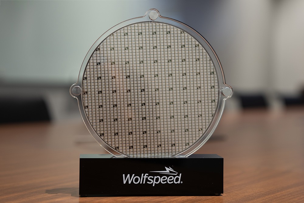
A stock image related to silicon carbide wafers.
The manufacturing process of silicon carbide (SiC) wafers is intricate and involves several key stages that ensure the production of high-quality substrates essential for various applications, particularly in power electronics and semiconductor devices. The main stages include:
Material Preparation:
- The process begins with the selection of high-purity silicon carbide crystals. These crystals are typically synthesized using methods such as the Lely method or modified Lely method, which involve sublimation of silicon and carbon at high temperatures.
- The selected crystals undergo a series of purification processes to eliminate impurities that could affect the wafer's electrical properties.
Forming the Wafers:
- Once purified, the SiC crystals are sliced into wafers using precision diamond saws. This step is crucial as it determines the thickness and flatness of the wafers.
- Wafers are typically cut into standard sizes such as 4-inch, 6-inch, and 8-inch diameters, depending on the specific application requirements.
Assembly:
- After slicing, the wafers undergo a cleaning process to remove any contaminants from the surface. This is usually done using a combination of ultrasonic cleaning and chemical treatments.
- The wafers are then inspected for defects, such as cracks or surface irregularities, which are critical for ensuring the performance of semiconductor devices.
Finishing:
- The final stage involves polishing the wafers to achieve the desired surface roughness and flatness. Polishing is essential as it prepares the surface for subsequent processes, such as epitaxy or device fabrication.
- A chemical-mechanical polishing (CMP) technique is often employed to achieve a high-quality finish.
The production of silicon carbide wafers leverages several advanced techniques to enhance quality and efficiency:
Epitaxial Growth: This process involves depositing thin layers of silicon carbide onto the wafer surface to improve its electrical characteristics. Techniques like CVD (Chemical Vapor Deposition) are commonly used.
Doping: To modify the electrical properties of the wafers, dopants are introduced during the epitaxial growth. This is crucial for tailoring the conductivity of the final product for specific applications.
Metrology and Characterization: Advanced tools such as atomic force microscopy (AFM) and X-ray diffraction (XRD) are employed to measure the physical and structural properties of the wafers, ensuring they meet stringent specifications.
Quality assurance (QA) is a critical component in the silicon carbide wafer production process. Adhering to international standards ensures that the wafers produced are reliable and meet the needs of B2B buyers.
International Standards:
- Compliance with standards such as ISO 9001 for quality management systems is essential. This certification indicates that the manufacturer has established a robust quality management process.
- Industry-specific certifications, such as CE marking for European markets and API (American Petroleum Institute) standards for energy applications, are also crucial for ensuring product quality.
Quality Control Checkpoints:
- Incoming Quality Control (IQC): This involves inspecting raw materials and components before they enter the production process.
- In-Process Quality Control (IPQC): Continuous monitoring during manufacturing helps identify defects early. Techniques like visual inspections and automated measurements are commonly used.
- Final Quality Control (FQC): Before shipment, wafers undergo rigorous testing to ensure they meet the required specifications. This includes electrical testing, surface roughness assessments, and defect inspections.
Common Testing Methods:
- Electrical tests, such as resistivity and breakdown voltage tests, are conducted to verify the electrical properties of the wafers.
- Surface analysis methods, including scanning electron microscopy (SEM), are employed to assess surface defects and morphology.
For international B2B buyers, particularly those from Africa, South America, the Middle East, and Europe, verifying the quality control processes of suppliers is vital for ensuring product reliability.
Supplier Audits: Conducting on-site audits of the manufacturing facility allows buyers to assess compliance with quality standards and evaluate the overall manufacturing environment.
Quality Reports: Requesting detailed quality reports and certifications from suppliers can provide insights into their quality management practices and adherence to international standards.
Third-Party Inspections: Engaging third-party inspection agencies can offer an unbiased assessment of the supplier’s quality control processes, ensuring that the products meet the required specifications before shipment.
Understanding the nuances of quality control in the silicon carbide wafer industry is crucial for international buyers:
Regulatory Compliance: Different regions have varying regulatory requirements. Buyers from the EU, for instance, must ensure that suppliers comply with REACH (Registration, Evaluation, Authorisation and Restriction of Chemicals) regulations.
Cultural Differences: Buyers should be aware of cultural differences that may affect communication and negotiation with suppliers. Building strong relationships can facilitate better quality assurance practices.
Logistics and Shipping: International shipping introduces additional quality assurance challenges. Buyers must ensure that the packaging and transportation methods protect the wafers from damage during transit.
By thoroughly understanding the manufacturing processes and quality assurance protocols, international B2B buyers can make informed decisions when sourcing silicon carbide wafers, ensuring they receive high-quality products that meet their specific needs.
This practical sourcing guide is designed to assist international B2B buyers in navigating the procurement of silicon carbide wafers. With the increasing demand for high-performance materials in various industries, understanding the sourcing process is essential for making informed decisions. This checklist will outline key steps to ensure you select the right suppliers and products to meet your technical and business needs.
Start by clearly outlining the specifications required for your silicon carbide wafers. This includes parameters such as diameter, thickness, crystal orientation, and doping type.
- Why It Matters: Having precise specifications helps in communicating your requirements effectively to suppliers, ensuring you receive products that meet your performance criteria.
- What to Look For: Make sure to reference industry standards relevant to your application, whether it's for power electronics, automotive, or high-frequency devices.
Conduct thorough research to identify potential suppliers of silicon carbide wafers. Utilize industry directories, trade shows, and online platforms to gather a list of candidates.
- Why It Matters: A broad search increases your chances of finding suppliers who offer competitive pricing and superior quality.
- What to Look For: Focus on suppliers with a proven track record, positive customer reviews, and expertise in silicon carbide technology.
Ensure that your shortlisted suppliers hold relevant certifications such as ISO 9001 or specific semiconductor industry certifications.
- Why It Matters: Certifications indicate a commitment to quality and adherence to industry standards, which can significantly reduce risks associated with product defects.
- What to Look For: Request documentation of certifications and assess whether they are current and applicable to silicon carbide wafer production.
Before making a bulk purchase, request samples of the silicon carbide wafers to evaluate their quality and performance in your specific application.
- Why It Matters: Testing samples allows you to assess whether the product meets your specifications and performance expectations without committing to a large order.
- What to Look For: Pay attention to parameters such as surface roughness, crystal defects, and electrical characteristics during your evaluation.
Analyze the pricing structures and payment terms from each supplier. Consider factors such as bulk order discounts, shipping costs, and payment flexibility.
- Why It Matters: Understanding the total cost of ownership helps you budget effectively and negotiate favorable terms.
- What to Look For: Look for transparent pricing without hidden fees and consider the financial stability of the supplier to ensure they can meet your long-term needs.
Investigate the lead times for order fulfillment and the supplier’s logistics capabilities. Ensure they can meet your production schedules without delays.
- Why It Matters: Delays in supply can disrupt your production processes and lead to increased costs.
- What to Look For: Confirm the supplier’s ability to handle international shipping and customs clearance, especially if you are sourcing from different continents.
Develop a communication plan to maintain ongoing dialogue with your chosen supplier. This should include regular updates on order status, product changes, and technical support.
- Why It Matters: Clear communication fosters a strong relationship, ensuring any issues are addressed promptly and effectively.
- What to Look For: Set expectations for response times and preferred communication channels to ensure smooth interactions.
By following this checklist, B2B buyers can effectively navigate the complexities of sourcing silicon carbide wafers, ensuring they make informed decisions that support their operational goals.
When sourcing silicon carbide wafers, understanding the cost structure is essential for making informed purchasing decisions. The primary cost components include:
Materials: The cost of raw silicon carbide crystals can fluctuate based on market demand and availability. High-purity materials are essential for quality wafers, and sourcing from reputable suppliers can ensure consistency.
Labor: Labor costs involve skilled technicians and engineers who handle the fabrication process. The complexity of silicon carbide manufacturing often necessitates specialized skills, which can impact pricing.
Manufacturing Overhead: This includes the costs associated with maintaining production facilities, utilities, and equipment depreciation. Advanced manufacturing technologies can enhance efficiency but may also increase initial costs.
Tooling: The creation and maintenance of specialized tools and molds for wafer production can add to costs. Custom tooling may be required for unique specifications, affecting the overall price.
Quality Control (QC): Rigorous QC processes are vital in ensuring the wafers meet industry standards. Investing in quality assurance can lead to higher upfront costs but can save money in the long run by reducing waste and defects.
Logistics: Transportation and shipping costs, including customs duties for international buyers, can significantly impact the total cost. Efficient logistics planning is crucial, particularly for buyers in regions like Africa and South America where infrastructure may vary.
Margin: Suppliers typically add a margin to cover their operational costs and profit. This margin can vary based on competition and market conditions.
Several factors can influence the pricing of silicon carbide wafers, including:
Volume/MOQ: The minimum order quantity (MOQ) can affect pricing. Larger orders often come with volume discounts, making it essential for buyers to assess their needs accurately.
Specifications and Customization: Customized wafers tailored to specific applications may incur higher costs. Detailed specifications can lead to increased production complexity, impacting pricing.
Material Quality and Certifications: Wafers with higher quality standards or certifications (like ISO or RoHS compliance) typically command higher prices. Buyers should weigh the importance of these certifications against their budget.
Supplier Factors: The reputation, location, and reliability of the supplier can influence costs. Established suppliers may charge premium prices for their products due to their proven track record.
Incoterms: Understanding Incoterms (International Commercial Terms) is crucial for international transactions. These terms dictate the responsibilities of buyers and sellers regarding shipping, insurance, and tariffs, impacting overall costs.
B2B buyers, especially from Africa, South America, the Middle East, and Europe, can leverage several strategies to optimize their sourcing process:
Negotiate Wisely: Engage in negotiations with suppliers to secure better pricing, especially when purchasing in bulk. Understanding the supplier’s cost structure can provide leverage during discussions.
Consider Total Cost of Ownership (TCO): Instead of focusing solely on the purchase price, evaluate the TCO, which includes shipping, handling, and potential future costs related to quality and performance. A lower upfront cost might lead to higher long-term expenses.
Understand Pricing Nuances: International buyers should be aware of local market conditions and currency fluctuations that can affect pricing. Establishing long-term relationships with suppliers can also lead to more favorable terms.
Research Suppliers Thoroughly: Due diligence is key. Assess suppliers' certifications, track records, and reviews from other B2B buyers to ensure reliability and quality.
Pricing for silicon carbide wafers can vary significantly based on the factors discussed above. The prices mentioned here are indicative and can change based on market conditions, supplier negotiations, and specific buyer requirements. Always seek updated quotes from suppliers before finalizing any orders.
When considering silicon carbide (SiC) wafers for various industrial applications, it's essential to explore viable alternatives. Each technology offers unique advantages and disadvantages that can significantly impact performance, cost, and overall suitability for specific projects. This section will provide a comprehensive comparison of silicon carbide wafers against two notable alternatives: gallium nitride (GaN) wafers and traditional silicon wafers.
| Comparison Aspect | Silicon Carbide Wafers | Gallium Nitride Wafers | Traditional Silicon Wafers |
|---|---|---|---|
| Performance | High thermal conductivity and efficiency | Superior efficiency in high-frequency applications | Adequate for low-power applications |
| Cost | Higher initial investment | Moderate costs, but increasing | Lower initial costs |
| Ease of Implementation | Requires specialized processes | More complex than silicon, but easier than SiC | Well-established manufacturing processes |
| Maintenance | Generally low maintenance | Moderate; can require special handling | Low maintenance |
| Best Use Case | High-power, high-temperature applications | RF and microwave applications | General-purpose applications |
Gallium nitride (GaN) wafers are known for their exceptional efficiency, particularly in high-frequency and high-power applications. They excel in environments where thermal management is critical, making them suitable for RF amplifiers and power converters. However, GaN wafers can be more challenging to manufacture compared to silicon, leading to a moderately higher cost. The complexity of GaN technology may require specialized training for personnel, impacting the ease of implementation.
Traditional silicon wafers have been the cornerstone of semiconductor technology for decades. They are cost-effective and have a well-established manufacturing infrastructure, which makes them the go-to choice for many general-purpose applications. However, their performance in high-temperature and high-power scenarios is limited compared to silicon carbide wafers. While they offer lower initial costs and ease of production, their efficiency and thermal performance may not meet the demands of advanced applications, leading to increased energy costs over time.
In selecting the appropriate wafer technology, B2B buyers must consider their specific application requirements, including power, efficiency, and thermal management. Silicon carbide wafers are ideal for high-performance environments that demand robust thermal management and efficiency. On the other hand, gallium nitride wafers may be preferable for applications requiring high-frequency operation but come with a more complex implementation process. Traditional silicon wafers remain a viable option for cost-sensitive projects where performance needs are moderate. By carefully evaluating these factors, buyers can make informed decisions that align with their operational goals and budget constraints.
A stock image related to silicon carbide wafers.
Understanding the technical properties of silicon carbide (SiC) wafers is essential for international B2B buyers, especially those in regions like Africa, South America, the Middle East, and Europe. Below are some critical specifications to consider when assessing silicon carbide wafers for various applications.
Silicon carbide wafers are categorized based on their material grades, which significantly impact their performance. Higher purity levels (e.g., 4H-SiC, 6H-SiC) indicate fewer impurities, leading to improved electronic characteristics and enhanced thermal conductivity. For B2B buyers, selecting the right material grade is crucial for ensuring device reliability and performance in high-temperature applications.
Tolerance refers to the acceptable deviation from specified dimensions of the wafer. Common thickness specifications range from 150 µm to 500 µm. High-precision tolerances are critical for applications in power electronics and optoelectronics, where even minor discrepancies can lead to significant operational issues. Buyers must ensure that the supplier can meet their specific tolerance requirements to avoid complications during manufacturing.
Surface roughness is a key indicator of wafer quality. Lower roughness values (measured in nanometers) are desirable, as they contribute to better device performance and yield in semiconductor fabrication. For B2B buyers, understanding surface roughness specifications can help in selecting wafers that enhance production efficiency and reduce waste.
Doping refers to the intentional introduction of impurities into the silicon carbide crystal structure to modify its electrical properties. Common dopants include nitrogen and phosphorus, which create n-type and p-type materials, respectively. Buyers need to specify the required doping levels based on the intended application, as this will influence the electrical performance of the end product.
Navigating the trade landscape for silicon carbide wafers requires familiarity with specific jargon. Here are some common terms that B2B buyers should understand:
An OEM is a company that manufactures products or components that are purchased by another company and sold under that company’s brand name. When sourcing silicon carbide wafers, buyers often engage with OEMs that specialize in semiconductor materials, which can lead to tailored solutions for specific applications.
MOQ refers to the minimum quantity of units a supplier is willing to sell. Understanding MOQ is vital for B2B buyers, as it can impact inventory management and cash flow. Buyers should negotiate MOQs that align with their production needs without overcommitting resources.
An RFQ is a document issued by buyers to solicit price quotes from suppliers for specific products or services. When purchasing silicon carbide wafers, issuing an RFQ helps buyers compare pricing, lead times, and terms from multiple vendors, enabling informed decision-making.
Incoterms are standardized trade terms that define the responsibilities of buyers and sellers in international transactions. Familiarity with terms like FOB (Free on Board) or CIF (Cost, Insurance, and Freight) is crucial for B2B buyers to understand shipping costs, risk transfer, and delivery obligations.
By grasping these essential properties and trade terms, international B2B buyers can make more informed decisions when sourcing silicon carbide wafers, ensuring they select the best options for their specific applications and operational needs.
The silicon carbide (SiC) wafers market is experiencing significant growth, driven primarily by the increasing demand for high-performance semiconductors in sectors such as automotive, telecommunications, and renewable energy. The shift towards electric vehicles (EVs) is a major catalyst, as SiC wafers enhance the efficiency and performance of power electronics used in these vehicles. Furthermore, the ongoing global push for renewable energy solutions, such as solar inverters and wind turbines, is propelling the adoption of SiC technology due to its superior thermal conductivity and efficiency compared to traditional silicon.
Emerging trends in B2B sourcing include a focus on supplier diversification and the establishment of long-term partnerships to mitigate risks associated with geopolitical tensions and supply chain disruptions. International buyers from regions like Africa, South America, the Middle East, and Europe, particularly in countries such as Spain and the UAE, are increasingly looking for suppliers who can offer not only competitive pricing but also reliability and quality assurance. Another trend is the integration of advanced manufacturing technologies, such as automation and AI, which enhance the production capabilities of SiC wafers and reduce lead times.
Sustainability is becoming a critical factor for B2B buyers in the silicon carbide wafers sector. The environmental impact of semiconductor manufacturing processes has raised concerns, prompting companies to seek sustainable practices within their supply chains. Ethical sourcing of raw materials, such as silicon carbide, is vital for companies aiming to meet regulatory standards and consumer expectations regarding sustainability.
Buyers are increasingly interested in suppliers that hold 'green' certifications, such as ISO 14001 for environmental management systems, which demonstrate a commitment to minimizing environmental impact. Additionally, the use of recycled materials and sustainable production methods is gaining traction, providing buyers with options that align with their sustainability goals. By prioritizing suppliers who adopt environmentally friendly practices, international buyers can enhance their brand reputation and meet the growing demand for sustainable products in their respective markets.
The evolution of silicon carbide wafers has been marked by significant technological advancements since their inception. Initially developed for high-temperature and high-power applications, SiC technology has matured over the years, leading to a broader range of applications across various industries. The introduction of advanced manufacturing techniques, such as epitaxial growth and improved crystal quality, has enhanced the performance and reliability of SiC wafers, making them a preferred choice for power electronics.
For B2B buyers, understanding this evolution is crucial as it informs their sourcing strategies and investment decisions. The continuous improvement in SiC wafer technology not only promises higher efficiency and performance but also supports the growing demand for greener and more sustainable solutions in the semiconductor industry. As a result, international buyers can leverage these advancements to gain a competitive edge in their markets while contributing to a more sustainable future.
1. How do I choose the right silicon carbide wafer supplier for my business?
Choosing the right silicon carbide wafer supplier involves evaluating several key factors. First, assess the supplier's experience and reputation in the industry. Look for companies with a proven track record in quality and reliability. Additionally, inquire about their manufacturing capabilities, certifications (like ISO), and whether they offer customization options to meet your specific needs. Finally, consider their customer service and responsiveness, as these can significantly impact your purchasing experience and ongoing support.
2. What are the typical payment terms for purchasing silicon carbide wafers in international trade?
Payment terms can vary widely among suppliers, but common practices include payment in advance, letters of credit, and net 30 or 60 days after delivery. For international transactions, it's advisable to negotiate terms that protect your interests while ensuring the supplier feels secure. Using an escrow service can also mitigate risks for both parties. Always clarify payment terms in the contract to avoid misunderstandings and ensure compliance with local regulations.
3. What is the minimum order quantity (MOQ) for silicon carbide wafers?
Minimum order quantities for silicon carbide wafers can differ based on the supplier and the specific wafer specifications. Generally, MOQs can range from a few pieces to several hundred. It's essential to communicate your requirements upfront to gauge the supplier's flexibility. Some suppliers may offer lower MOQs for first-time buyers or larger orders, while others might have strict policies. Always verify MOQs to plan your procurement strategy effectively.
4. How can I ensure quality assurance when sourcing silicon carbide wafers?
To ensure quality assurance, request detailed information about the supplier's quality control processes. Look for certifications such as ISO 9001 or specific industry standards relevant to silicon carbide wafers. Ask for documentation of batch testing results and inspection processes. Additionally, consider requesting samples before placing a large order to evaluate the quality firsthand. Establishing a clear quality agreement in your contract can also help maintain standards throughout the production process.
5. What logistics considerations should I keep in mind when importing silicon carbide wafers?
When importing silicon carbide wafers, consider shipping methods, lead times, and customs regulations. Air freight is faster but more expensive, while sea freight offers cost savings but longer transit times. Ensure your supplier can provide the necessary shipping documentation, including invoices and customs declarations. Familiarize yourself with import duties and taxes in your country to avoid unexpected costs. Collaborating with a reliable freight forwarder can streamline the logistics process and ensure compliance with all regulations.
6. How do I customize silicon carbide wafers for specific applications?
Customizing silicon carbide wafers typically involves specifying parameters like thickness, diameter, doping levels, and surface finish. Communicate your specific application requirements clearly to the supplier, as they may have the capability to tailor their products to meet your needs. It’s also beneficial to consult with the supplier's technical team for recommendations and feasibility assessments. Be prepared for potential additional costs and lead times associated with custom orders.
7. What are the common applications for silicon carbide wafers in various industries?
Silicon carbide wafers are utilized in numerous applications, notably in power electronics, high-temperature environments, and RF devices. Industries such as automotive (for electric vehicles), telecommunications, and renewable energy rely on silicon carbide for its superior thermal conductivity and efficiency. Understanding the specific requirements of your industry can help you determine the right specifications for your silicon carbide wafers, enhancing performance and reliability in your applications.
8. How can I verify the credibility of a silicon carbide wafer supplier before placing an order?
To verify a supplier's credibility, conduct thorough research on their business history, customer reviews, and industry certifications. Request references from previous clients to gain insights into their experiences. Utilize platforms like LinkedIn to check for professional endorsements and connections within the industry. Additionally, consider visiting the supplier's facility if feasible or arranging a virtual tour to assess their operations and quality control practices. A credible supplier should be transparent and willing to provide the information you need.
The information provided in this guide, including content regarding manufacturers, technical specifications, and market analysis, is for informational and educational purposes only. It does not constitute professional procurement advice, financial advice, or legal advice.
While we have made every effort to ensure the accuracy and timeliness of the information, we are not responsible for any errors, omissions, or outdated information. Market conditions, company details, and technical standards are subject to change.
B2B buyers must conduct their own independent and thorough due diligence before making any purchasing decisions. This includes contacting suppliers directly, verifying certifications, requesting samples, and seeking professional consultation. The risk of relying on any information in this guide is borne solely by the reader.
In the rapidly evolving landscape of silicon carbide (SiC) wafers, strategic sourcing emerges as a critical component for international B2B buyers. This material, known for its superior thermal and electrical properties, is essential for applications in high-efficiency power devices, electric vehicles, and renewable energy systems. By leveraging strategic sourcing, companies can not only optimize their supply chains but also secure competitive pricing and ensure the reliability of their SiC wafer supply.
For buyers in Africa, South America, the Middle East, and Europe, particularly in markets like Spain and the UAE, establishing partnerships with reputable manufacturers is vital. Engaging with suppliers who prioritize sustainability and innovation can provide long-term advantages, including access to cutting-edge technologies and enhanced product quality.
Looking ahead, as the demand for silicon carbide continues to surge, now is the time to reassess your sourcing strategies. Embrace the opportunities within this market by fostering relationships with suppliers who can meet your evolving needs. By doing so, you position your business not only for immediate gains but also for future growth in a technology-driven world.
Tags: Black Silicon Carbide, White Fused Alumina, Brown Fused Alumina, Pink Fused Alumina, Black Fused Alumina