Silicon carbide (SiC) wafers are at the forefront of innovation in semiconductor technology, powering critical applications in electric vehicles, renewable energy, telecommunications, and high-frequency electronics. For international B2B buyers—particularly those operating in dynamic markets across Africa, South America, the Middle East, and Europe—securing reliable, high-quality silicon carbide wafer suppliers is essential to maintaining competitive advantage and meeting stringent industry standards.
This guide offers a comprehensive roadmap designed to empower procurement professionals and technical decision-makers with actionable insights into the global silicon carbide wafer supply landscape. It delves into the various types and specifications of SiC wafers, elucidates the materials and manufacturing processes that define quality and performance, and highlights critical quality control measures that ensure consistency and reliability.
Illustrative Image (Source: Google Search)
Beyond technical details, the guide provides an in-depth analysis of key global suppliers, evaluating their capabilities and geographic reach to help buyers identify partners that align with their strategic sourcing goals. It also addresses cost considerations, including pricing dynamics and value optimization strategies, while offering an overview of current market trends shaping supply and demand.
For B2B buyers from emerging and established markets alike—such as Kenya, Brazil, the UAE, and Germany—this resource is tailored to facilitate informed decision-making, reduce procurement risks, and foster sustainable supplier relationships. Whether you are entering the silicon carbide wafer market or seeking to optimize your existing supply chain, this guide equips you with the knowledge necessary to navigate complexities and capitalize on opportunities in this rapidly evolving sector.
| Type Name | Key Distinguishing Features | Primary B2B Applications | Brief Pros & Cons for Buyers |
|---|---|---|---|
| Bulk Crystal Silicon Carbide Suppliers | Provide raw, large-diameter SiC boules for wafer slicing | Semiconductor fabrication, power electronics | + Custom sizes, cost-effective for large volumes – Longer lead times, requires in-house slicing capabilities |
| Processed Wafer Suppliers | Deliver polished, ready-to-use wafers with specific orientations and doping | High-precision electronics, RF devices | + Ready for immediate use, consistent quality – Higher unit cost, limited customization post-purchase |
| Specialty Doped Silicon Carbide Suppliers | Offer wafers with tailored doping levels and electrical properties | High-power devices, sensors, and automotive electronics | + Enables advanced device design, enhanced performance – Niche market, potentially higher prices and MOQ |
| Small-Scale/Custom Order Suppliers | Focus on small batch or custom specifications for R&D or niche applications | Research institutions, prototyping, specialized electronics | + Flexible order sizes, fast turnaround – Higher per-unit cost, limited scalability |
| Integrated Supply Chain Suppliers | Provide end-to-end solutions including wafer production, testing, and packaging | Large-scale manufacturers requiring supply chain reliability | + Streamlined procurement, quality assurance – May require long-term contracts, less price flexibility |
Bulk Crystal Silicon Carbide Suppliers specialize in producing large-diameter SiC boules from which wafers are sliced. These suppliers are ideal for manufacturers with in-house wafer processing capabilities who need custom sizes or large volumes. Buyers from regions like Africa or South America benefit from cost efficiencies but must factor in longer lead times and logistics for raw material handling. Evaluating supplier consistency and boule quality is critical to ensure downstream device performance.
Processed Wafer Suppliers provide wafers that have been polished, oriented, and sometimes doped, ready for immediate integration into semiconductor fabrication lines. This type suits B2B buyers seeking to reduce processing complexity and time-to-market, especially in Europe and the Middle East where high-precision electronics production is prominent. The trade-off is a higher per-unit cost and limited ability to customize wafers after purchase, making upfront specification accuracy vital.
Specialty Doped Silicon Carbide Suppliers focus on wafers with specific doping profiles and electrical characteristics tailored for high-power or sensor applications. These suppliers are essential for automotive, aerospace, and industrial electronics sectors that demand enhanced device performance. Buyers must consider minimum order quantities and price premiums but gain access to wafers that enable advanced device innovation and differentiation.
Small-Scale/Custom Order Suppliers cater primarily to research institutions, startups, and niche manufacturers requiring small batches or unique specifications. This flexibility supports rapid prototyping and specialized applications, making them attractive to R&D buyers in emerging markets like Kenya or specialized European tech hubs. However, costs per wafer are higher, and scalability is limited, so these suppliers are best for development phases rather than mass production.
Integrated Supply Chain Suppliers offer comprehensive solutions that include wafer production, testing, and packaging, appealing to large-scale manufacturers demanding supply chain reliability and quality assurance. These suppliers often serve multinational corporations with stringent procurement standards, common in the Middle East and Europe. While they streamline operations and reduce vendor complexity, buyers should be prepared for longer contractual commitments and potentially less price negotiation flexibility.
Related Video: Silicon carbide wafer thinning
| Industry/Sector | Specific Application of silicon carbide wafer suppliers | Value/Benefit for the Business | Key Sourcing Considerations for this Application |
|---|---|---|---|
| Power Electronics | High-voltage power devices for electric vehicles and renewable energy systems | Enhanced energy efficiency and thermal performance, reducing losses and improving device lifespan | Consistent wafer quality, high crystal purity, and supplier capacity to meet volume demands for scaling production |
| Semiconductor Manufacturing | Fabrication of high-frequency, high-temperature electronic components | Enables miniaturization and improved performance of semiconductors, supporting advanced electronics | Availability of wafers with precise doping and defect control, plus reliable logistics for international buyers |
| Renewable Energy | Silicon carbide wafers for inverters and converters in solar and wind energy | Improved conversion efficiency and durability in harsh environmental conditions | Suppliers with certifications for environmental compliance and ability to deliver to remote or emerging markets |
| Industrial Automation | Components in motor drives and robotics requiring high power density | Increased operational efficiency and reduced downtime through robust, heat-resistant wafers | Flexibility in wafer specifications and strong technical support for integration into complex systems |
| Telecommunications | RF and microwave devices for 5G infrastructure and satellite communications | Superior signal integrity and power handling at high frequencies | Consistent wafer uniformity and supplier expertise in high-frequency applications |
Silicon carbide wafers are pivotal in power electronics, particularly for electric vehicles and renewable energy infrastructures such as solar inverters and wind turbines. These wafers facilitate devices that operate at higher voltages and temperatures than traditional silicon, drastically improving energy efficiency and device longevity. Buyers from regions like Africa and South America should prioritize suppliers who can guarantee high crystal purity and stable supply chains to support growing energy transition projects.
In semiconductor manufacturing, silicon carbide wafers enable the production of advanced electronic components that require high-frequency operation and thermal stability. This is crucial for industries pushing the boundaries of miniaturization and performance. International buyers, especially from Europe and the Middle East, must ensure suppliers provide wafers with tight doping control and minimal defects to meet stringent performance standards.
The renewable energy sector benefits significantly from silicon carbide wafers used in power converters and inverters. These components must withstand harsh environmental conditions, offering increased reliability and efficiency. For buyers in emerging markets such as Kenya or Australia, sourcing from suppliers with environmental compliance certifications and robust logistics networks is essential to ensure timely delivery and adherence to sustainability goals.
In industrial automation, silicon carbide wafers are integral to motor drives and robotics that demand high power density and thermal resilience. This application reduces operational downtime and boosts efficiency. Buyers should seek suppliers offering customization and technical support, facilitating seamless integration into complex automation systems prevalent in modern manufacturing hubs across South America and Europe.
Lastly, in telecommunications, silicon carbide wafers support RF and microwave devices critical for 5G infrastructure and satellite communication. These wafers provide superior signal integrity and power handling. For international B2B buyers, consistent wafer uniformity and supplier expertise in high-frequency applications are key to maintaining network reliability and advancing telecommunications capabilities in their regions.
Related Video: What is Silicon Carbide?
When sourcing silicon carbide wafers, understanding the substrate materials is critical to align product performance with end-use requirements. Below is an analysis of the most common silicon carbide wafer materials from a B2B perspective, emphasizing their properties, advantages, limitations, and regional procurement considerations.
Key Properties:
4H-SiC is characterized by a wide bandgap (~3.26 eV), high thermal conductivity (~4.9 W/cm·K), and excellent chemical stability. It supports high electron mobility and can withstand temperatures exceeding 600°C, making it ideal for high-power, high-frequency applications.
Pros & Cons:
- Pros: Superior electrical properties for power electronics, high thermal stability, excellent corrosion resistance, and compatibility with advanced semiconductor manufacturing processes.
- Cons: Higher production complexity and cost due to stringent crystal growth requirements; wafer sizes are typically smaller compared to other materials.
Impact on Application:
4H-SiC wafers are preferred in power devices, such as MOSFETs and Schottky diodes, used in electric vehicles, renewable energy systems, and aerospace electronics, where efficiency and thermal management are critical.
International Buyer Considerations:
Buyers from Africa, South America, the Middle East, and Europe should verify compliance with international standards such as ASTM F1856 and JEDEC JESD22 for electrical and mechanical properties. European buyers, especially in Germany and France, often require wafers that meet DIN standards for semiconductor fabrication. Import regulations and tariffs may affect cost and delivery timelines, particularly in regions like Kenya and Brazil. Establishing partnerships with suppliers offering robust after-sales technical support is advantageous.
Key Properties:
6H-SiC has a slightly narrower bandgap (~3.0 eV) and lower electron mobility than 4H-SiC but retains high thermal conductivity and chemical inertness. It can operate effectively at elevated temperatures and under harsh chemical environments.
Pros & Cons:
- Pros: Easier and less costly to produce than 4H-SiC, with good mechanical strength and chemical resistance.
- Cons: Lower electron mobility limits its use in high-frequency devices; less common in cutting-edge power electronics.
Impact on Application:
6H-SiC is suitable for high-temperature sensors, LED substrates, and some power devices where ultra-high electron mobility is not critical. Its robustness makes it a candidate for industrial applications involving corrosive media.
International Buyer Considerations:
Buyers in emerging markets should consider 6H-SiC when cost constraints are significant but performance requirements remain moderate. Compliance with ASTM F1856 and ISO semiconductor standards is typical. For Middle Eastern buyers, ensuring wafer compatibility with local environmental conditions (e.g., high dust and temperature fluctuations) is essential. Logistics providers with experience in handling fragile semiconductor materials can mitigate risks during shipment.
Key Properties:
3C-SiC (cubic polytype) offers a bandgap of ~2.36 eV and exhibits high electron mobility, but has lower thermal conductivity (~3.7 W/cm·K) compared to hexagonal polytypes. It is often grown on silicon substrates, enabling integration with silicon-based electronics.
Pros & Cons:
- Pros: Lower manufacturing cost due to compatibility with silicon substrates; potential for integration with existing silicon semiconductor processes.
- Cons: Lower thermal conductivity limits high-power applications; crystal quality and wafer size are often limited, affecting yield and scalability.
Impact on Application:
3C-SiC is advantageous in MEMS devices, optoelectronics, and low-power electronics where integration with silicon is beneficial. It is less suited for high-power or high-temperature applications.
International Buyer Considerations:
For buyers in regions like South America and Africa, 3C-SiC wafers can offer a cost-effective entry into SiC technology, especially for applications that do not require extreme thermal performance. Compliance with JIS and IEC semiconductor standards may be relevant for buyers in Australia and Europe. Due diligence on supplier quality certifications (e.g., ISO 9001) is recommended to ensure consistent wafer quality.
Key Properties:
Epitaxial layers are thin, high-purity SiC films grown on bulk SiC substrates (commonly 4H-SiC). They offer controlled doping profiles and superior surface quality essential for device fabrication.
Pros & Cons:
- Pros: Enables precise control over electrical properties, improves device performance, and reduces defect density.
- Cons: Adds complexity and cost to wafer production; requires advanced manufacturing capabilities.
Impact on Application:
Epitaxial SiC wafers are critical for high-performance power devices, RF components, and sensors. They are preferred where device uniformity and reliability are paramount.
International Buyer Considerations:
International buyers should assess supplier capabilities in epitaxial growth technology and verify process certifications. Compliance with ASTM and JEDEC standards ensures wafer consistency. For buyers in Europe and the Middle East, sourcing from suppliers with strong technical collaboration and support frameworks is beneficial to manage complex device fabrication processes.
| Material | Typical Use Case for silicon carbide wafer suppliers | Key Advantage | Key Disadvantage/Limitation | Relative Cost (Low/Med/High) |
|---|---|---|---|---|
| 4H-Silicon Carbide (4H-SiC) | High-power, high-frequency power electronics | Superior electrical performance and thermal stability | High production complexity and cost | High |
| 6H-Silicon Carbide (6H-SiC) | High-temperature sensors, LED substrates, industrial devices | Good mechanical strength and chemical resistance | Lower electron mobility limits advanced applications | Medium |
| 3C-Silicon Carbide (3C-SiC) | MEMS, optoelectronics, low-power integrated devices | Compatibility with silicon substrates reduces cost | Lower thermal conductivity and limited wafer size | Low |
| Epitaxial SiC Layers on SiC | High-performance power devices and RF components | Precise doping control and improved device uniformity | Increased manufacturing complexity and cost |
Silicon carbide (SiC) wafers are critical components in advanced semiconductor applications, especially in power electronics and high-temperature devices. Understanding the manufacturing process is essential for B2B buyers to assess supplier capabilities and product quality.
Illustrative Image (Source: Google Search)
1. Material Preparation
The process begins with the synthesis of high-purity silicon carbide crystals, typically through physical vapor transport (PVT) or chemical vapor deposition (CVD). Raw materials such as silicon and carbon sources undergo precise purification to minimize defects and impurities. The supplier’s ability to control material purity directly impacts wafer performance and reliability.
2. Crystal Growth and Wafer Formation
Once the SiC crystals are grown, they are sliced into thin wafers using diamond wire saws or laser cutting. The wafer thickness and surface flatness are tightly controlled to meet specific application requirements. Key techniques include:
3. Wafer Polishing and Finishing
Polishing is critical to achieve a mirror-like surface finish, essential for semiconductor device fabrication. Chemical-mechanical polishing (CMP) removes surface defects and achieves nanometer-scale flatness. Additional finishing processes may include:
4. Assembly and Packaging (if applicable)
For suppliers offering integrated solutions, wafer assembly into device-ready forms may follow. This stage involves die bonding, wire bonding, and encapsulation, though many suppliers focus solely on wafer production.
Robust quality assurance (QA) is fundamental for ensuring wafers meet stringent specifications demanded by semiconductor manufacturers. International B2B buyers should prioritize suppliers with comprehensive QA systems aligned with global standards.
International Quality Standards
- ISO 9001: The baseline for quality management systems, ensuring consistent process control and continuous improvement.
- Industry-Specific Certifications: For wafers used in automotive or aerospace sectors, certifications such as IATF 16949 (automotive) or AS9100 (aerospace) may apply.
- CE Marking: Relevant for wafers incorporated into products sold within the European Economic Area, indicating compliance with health, safety, and environmental protection standards.
- API Standards: For applications in oil & gas or energy sectors, API certifications may be relevant, reflecting industry-specific QA demands.
Quality control (QC) is implemented at multiple stages to detect defects early and ensure process consistency:
Silicon carbide wafers require rigorous testing to meet performance criteria:
For international buyers, especially from Africa, South America, the Middle East, and Europe, verifying supplier QA capabilities is critical to mitigate risks associated with product quality and delivery reliability.
1. On-Site Audits
Request supplier audits focusing on manufacturing processes, equipment calibration, and QC procedures. On-site visits provide firsthand insight into operational rigor and compliance with stated standards.
2. Review of Quality Documentation
Ask for certificates (ISO 9001, IATF 16949, CE), test reports, and traceability records. Transparent documentation demonstrates supplier commitment to quality and regulatory compliance.
3. Third-Party Inspections
Engage independent inspection agencies to conduct pre-shipment inspections and random sampling tests. This is especially useful for buyers in regions with less established semiconductor ecosystems, providing an unbiased quality verification layer.
4. Supplier Quality Agreements (SQA)
Negotiate detailed SQAs that define quality metrics, inspection frequencies, and corrective action protocols. SQAs formalize expectations and foster accountability.
Regional Regulatory Compliance: Buyers in Europe must ensure suppliers comply with REACH and RoHS directives, which restrict hazardous substances in electronic components. Middle Eastern and African buyers should verify compliance with local import regulations and certifications.
Logistics and Packaging: Silicon carbide wafers are sensitive to contamination and mechanical damage. Ensure suppliers use industry-standard cleanroom packaging and robust shipping methods to maintain wafer integrity during transit, especially for long-distance shipments to South America or Africa.
Supplier Localization and Support: Consider suppliers offering local or regional support centers to facilitate faster communication, technical assistance, and warranty services.
Custom Specifications: International buyers often have unique application requirements. Engage early with suppliers to confirm their capability to customize wafer dimensions, doping levels, and surface finishes, backed by rigorous QC.
For international B2B buyers sourcing silicon carbide wafers, a deep understanding of manufacturing processes and quality assurance protocols is indispensable. Evaluate suppliers based on their crystal growth expertise, precision wafer processing, adherence to international quality standards, and transparent QC practices. Verifying quality through audits, documentation, and third-party inspections safeguards your investment and ensures reliable supply chains across diverse markets including Africa, South America, the Middle East, and Europe.
Understanding the cost and pricing dynamics of silicon carbide (SiC) wafer suppliers is crucial for international B2B buyers aiming to optimize procurement strategies. The price of SiC wafers is influenced by a complex interplay of production costs, market conditions, and logistical considerations. Below is a detailed breakdown of the key cost components, pricing influencers, and actionable buyer tips tailored for stakeholders from regions including Africa, South America, the Middle East, and Europe.
Raw Materials
Silicon carbide wafers require high-purity silicon carbide crystals, which are costly due to the complex growth processes (e.g., Physical Vapor Transport). The quality and grade of the starting material significantly impact the final wafer price.
Labor Costs
Skilled labor is essential for crystal growth, slicing, polishing, and inspection. Labor costs vary by supplier location and can affect the overall wafer cost, especially when sourcing from regions with higher wage standards.
Manufacturing Overhead
Includes factory utilities, equipment depreciation, and maintenance. SiC wafer production demands high-tech equipment and cleanroom environments, which add to overhead costs.
Tooling and Equipment
Specialized machinery for wafer slicing, grinding, and polishing has high upfront costs and ongoing maintenance expenses, contributing to the unit cost of wafers.
Quality Control (QC)
Rigorous testing for defects, electrical properties, and surface quality is mandatory. QC processes increase cost but are critical for ensuring wafer reliability, especially for high-performance applications.
Logistics and Freight
International shipping, customs duties, and insurance add significant costs, particularly for buyers in Africa, South America, and the Middle East where transport infrastructure or customs processes may be less streamlined.
Supplier Margin
Profit margins vary depending on supplier strategy, market demand, and competitive positioning. Margins may tighten in highly competitive markets but widen for suppliers offering premium quality or niche specifications.
Order Volume and Minimum Order Quantity (MOQ)
Larger orders typically benefit from volume discounts. However, minimum order quantities can be restrictive, especially for smaller companies or those testing new suppliers.
Specifications and Customization
Higher-grade wafers with tighter tolerances, specific doping levels, or unique sizes command premium pricing. Customization increases tooling and QC costs.
Material Quality and Certification
Suppliers offering wafers with certifications such as ISO 9001, IATF 16949, or compliance with automotive-grade standards often price higher due to additional compliance costs.
Supplier Location and Reputation
Established suppliers in Asia, Europe, or North America may charge premiums for proven reliability, while emerging suppliers may offer competitive pricing but with higher risk.
Incoterms and Payment Terms
The choice of Incoterms (e.g., FOB, CIF, DDP) affects who bears shipping and customs costs. Payment terms (e.g., letter of credit, net 30/60) impact cash flow and potentially price negotiations.
Negotiate Beyond Unit Price
Engage suppliers on payment terms, lead times, and after-sales support. Favorable terms can reduce overall procurement costs.
Assess Total Cost of Ownership (TCO)
Factor in logistics, customs fees, potential tariffs, and inventory holding costs. For example, importing into Kenya or Brazil may involve higher customs duties and longer clearance times.
Leverage Regional Trade Agreements
Buyers in Europe or the Middle East should explore sourcing from countries with free trade agreements to reduce tariffs and improve delivery times.
Validate Supplier Certifications and Quality
Prioritize suppliers with internationally recognized quality certifications to mitigate risk and ensure product reliability, especially for critical applications.
Understand Pricing Nuances by Region
Logistics costs can significantly inflate prices in Africa or South America due to limited direct shipping routes. Consider consolidating shipments or using regional distributors to reduce costs.
Plan for MOQ Constraints
Where MOQs are high, consider pooling orders with other buyers or negotiating smaller trial batches to test quality before committing to large volumes.
Disclaimer: Prices for silicon carbide wafers can vary widely depending on specifications, supplier location, order size, and market conditions. The insights provided here are indicative and should be validated with direct supplier quotations and current market research.
Understanding the critical technical properties and common trade terminology related to silicon carbide (SiC) wafers is essential for B2B buyers, especially those navigating international procurement from regions such as Africa, South America, the Middle East, and Europe. This knowledge ensures informed decision-making, optimizes supply chain negotiations, and enhances communication with suppliers.
Material Grade (Polytype)
Silicon carbide wafers come in different polytypes, primarily 4H-SiC and 6H-SiC. The polytype affects the electrical characteristics, such as electron mobility and bandgap, which are critical for semiconductor performance. Buyers must specify the required polytype to ensure compatibility with their end-use applications, such as power electronics or high-frequency devices.
Wafer Diameter
Diameter typically ranges from 2 inches (50 mm) up to 6 inches (150 mm) or more. Larger diameters generally translate to higher production efficiency but may come with increased costs and handling complexity. Understanding wafer size is crucial for aligning with manufacturing equipment capabilities and cost optimization.
Thickness and Thickness Tolerance
The wafer thickness impacts device fabrication and mechanical stability. Tolerances often range within a few microns. Precise thickness control is vital to maintain uniformity across batches and to reduce material waste during processing, which directly influences yield and cost.
Crystallographic Orientation
Orientation, such as (0001) or (11-20), defines the wafer surface plane and affects epitaxial layer growth and device performance. Buyers should specify orientation to match their epitaxial growth processes and device design requirements.
Surface Finish and Polishing Quality
The surface roughness and polish level affect subsequent wafer processing steps like epitaxy and lithography. High-quality, defect-free surfaces minimize device failure rates and improve yield. Buyers should request detailed surface finish specifications, especially for high-precision applications.
Resistivity and Doping Level
Resistivity, influenced by doping concentration, determines the electrical properties of the wafer substrate. Precise control over these parameters is critical for device functionality. Buyers must ensure that the wafers meet the required resistivity range for their semiconductor devices.
OEM (Original Equipment Manufacturer)
Refers to companies that produce end products using silicon carbide wafers as components. Understanding whether a supplier works directly with OEMs can indicate the quality standards and reliability of their wafers.
MOQ (Minimum Order Quantity)
The smallest quantity a supplier is willing to sell in a single order. For international buyers, especially SMEs in emerging markets, negotiating MOQ is important to balance inventory costs and supply continuity.
RFQ (Request for Quotation)
A formal inquiry sent to suppliers to obtain pricing, lead times, and terms for silicon carbide wafers. Crafting detailed RFQs with clear technical specifications improves quote accuracy and supplier responsiveness.
Incoterms (International Commercial Terms)
Standardized trade terms (e.g., FOB, CIF, DDP) defining responsibilities for shipping, insurance, and customs clearance. Familiarity with Incoterms helps buyers manage logistics risks and costs effectively when importing wafers internationally.
Epitaxial Layer
A thin layer of silicon carbide grown on the wafer surface to create the active semiconductor region. Buyers should confirm compatibility between the wafer substrate and epitaxial layer specifications to ensure device performance.
Yield
The percentage of wafers or devices meeting quality standards after processing. Higher yield translates to better cost-efficiency. Buyers often seek suppliers with proven high yield rates to minimize production losses.
By mastering these technical properties and trade terms, international B2B buyers can better evaluate silicon carbide wafer suppliers, negotiate favorable terms, and ensure the wafers meet their application needs and quality standards. This knowledge is particularly valuable for buyers in diverse markets such as Africa, South America, the Middle East, and Europe, where supply chain complexities require clear, precise communication and strategic purchasing decisions.
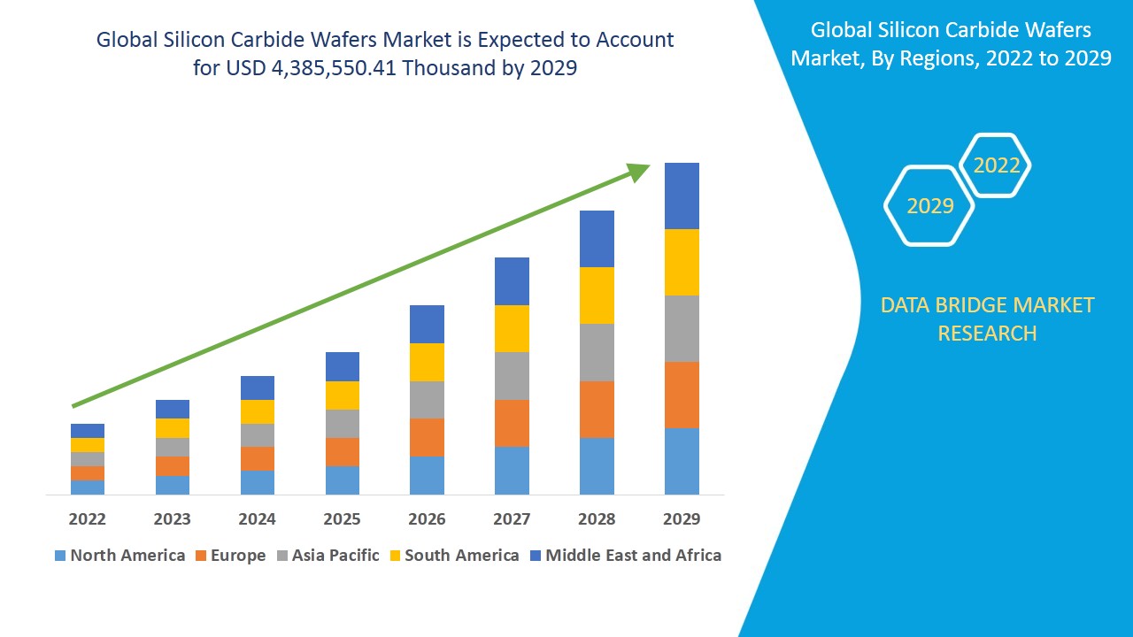
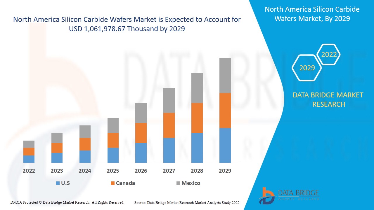
The silicon carbide (SiC) wafer market is experiencing robust growth driven by increasing demand in high-power electronics, electric vehicles (EVs), renewable energy systems, and industrial applications. For international B2B buyers from regions such as Africa, South America, the Middle East, and Europe, understanding these dynamics is crucial to securing competitive supply chains and leveraging technological advancements.
Key Market Drivers:
Emerging Sourcing Trends:
Market Dynamics for International Buyers:
By aligning procurement strategies with these trends, B2B buyers can secure resilient supply chains while accessing high-performance materials that meet evolving industry standards.
Sustainability is becoming a decisive factor in silicon carbide wafer procurement, especially for international buyers committed to corporate social responsibility and regulatory compliance. The production of SiC wafers involves energy-intensive processes and the use of specialized chemicals, which can have significant environmental impacts if not managed responsibly.
Illustrative Image (Source: Google Search)
Environmental Impact Considerations:
Importance of Ethical Supply Chains:
Green Certifications and Materials:
For B2B buyers, integrating sustainability criteria into supplier evaluation not only mitigates environmental risks but also enhances brand reputation and aligns with evolving customer expectations.
The silicon carbide wafer industry has evolved significantly since its inception in the 1950s when SiC was first recognized for its exceptional hardness and thermal properties. Initially, SiC wafers were niche products used primarily in abrasive applications and specialized electronics.
The 1990s marked a turning point with advancements in crystal growth techniques such as the Physical Vapor Transport (PVT) method, enabling larger and higher-quality SiC wafers. This evolution facilitated their adoption in power electronics, especially for high-voltage and high-frequency applications.
Over the past two decades, wafer diameters have increased from 50 mm to 150 mm and beyond, enhancing economies of scale and reducing per-unit costs. This has made SiC wafers more accessible to a broader range of industries, including automotive and renewable energy sectors.
For B2B buyers, understanding this historical context highlights the importance of engaging with suppliers who continuously innovate in wafer technology, ensuring access to materials that meet the stringent performance and reliability demands of modern electronic devices.
1. How can I effectively vet silicon carbide wafer suppliers for international B2B transactions?
Start by evaluating the supplier’s industry certifications, such as ISO 9001 for quality management and any specific semiconductor manufacturing standards. Request samples and technical datasheets to verify product quality and consistency. Check references and customer testimonials, especially from buyers in your region. Assess their financial stability and capacity to meet your order volume. Additionally, confirm their compliance with international trade regulations and export capabilities, ensuring smooth customs clearance and timely deliveries.
2. What customization options are typically available for silicon carbide wafers, and how can I communicate my specific needs?
Most suppliers offer customization in terms of wafer diameter, thickness, doping concentration, crystal orientation, and surface finish. Clearly specify your technical requirements in writing, including tolerance levels and intended application. Engage in detailed technical discussions with the supplier’s engineering team to ensure feasibility. Request prototypes or small trial orders to validate specifications before full-scale procurement. Establishing clear communication channels and using technical drawings or standards can minimize misunderstandings.
3. What are the common minimum order quantities (MOQs) and lead times for silicon carbide wafers, and how do they vary by region?
MOQs can range from a few dozen to several hundred wafers, depending on supplier capacity and wafer specifications. Lead times typically span 6 to 12 weeks but can extend due to customization or supply chain disruptions. Buyers in Africa, South America, and the Middle East should factor in additional time for logistics and customs clearance. Negotiate flexible MOQs when possible, especially for first orders, and establish clear timelines in contracts to align expectations and production schedules.
4. Which payment terms are standard in international B2B deals for silicon carbide wafers, and how can buyers mitigate financial risks?
Common payment terms include letters of credit (LC), wire transfers, and escrow services. Letters of credit offer protection by guaranteeing payment upon shipment verification, ideal for first-time transactions. For established relationships, net payment terms (e.g., 30-60 days) may be negotiated. To mitigate risks, conduct due diligence on supplier credibility, use trade finance instruments, and consider partial upfront payments combined with balance upon delivery. Ensure all terms are clearly outlined in the purchase agreement.
5. How important are quality assurance (QA) processes and certifications when selecting a silicon carbide wafer supplier?
QA processes and certifications are critical indicators of product reliability and supplier professionalism. Look for suppliers with documented process controls, in-line inspections, and final product testing. Certifications like ISO 9001, IATF 16949 (automotive), or industry-specific standards provide assurance of consistent quality. Request detailed QA reports and traceability documentation for each batch. This is especially important for buyers in regulated markets such as Europe and the Middle East, where compliance with safety and environmental standards is mandatory.
6. What logistics considerations should international buyers be aware of when importing silicon carbide wafers?
Silicon carbide wafers are delicate and require specialized packaging to prevent contamination and physical damage during transit. Confirm that the supplier uses industry-standard packaging materials and handling protocols. Understand import regulations, tariffs, and customs procedures in your country to avoid delays. Work with freight forwarders experienced in semiconductor shipments and consider insurance coverage for high-value goods. Planning for potential delays and having contingency plans can help maintain your production schedules.
7. How should disputes or quality issues be handled with silicon carbide wafer suppliers in cross-border transactions?
Establish clear dispute resolution mechanisms in your contract, such as arbitration clauses or jurisdiction agreements. Promptly document and communicate any quality concerns with detailed evidence, including photos and test results. Engage the supplier in collaborative problem-solving to identify root causes and corrective actions. Retain third-party inspection or testing services if necessary. Building a transparent and cooperative relationship helps resolve issues efficiently and maintains long-term partnerships.
8. Are there regional differences in supplier reliability or support services that B2B buyers should consider?
Yes, supplier reliability and after-sales support can vary significantly by region. Suppliers in Europe often provide robust technical support and adherence to stringent quality standards, while those in emerging markets may offer competitive pricing but require more thorough vetting. For buyers in Africa and South America, partnering with suppliers who have established local distributors or service centers can improve responsiveness. Assess the supplier’s language capabilities, time zone alignment, and willingness to provide training or on-site assistance to ensure smooth collaboration.
The information provided in this guide, including content regarding manufacturers, technical specifications, and market analysis, is for informational and educational purposes only. It does not constitute professional procurement advice, financial advice, or legal advice.
While we have made every effort to ensure the accuracy and timeliness of the information, we are not responsible for any errors, omissions, or outdated information. Market conditions, company details, and technical standards are subject to change.
B2B buyers must conduct their own independent and thorough due diligence before making any purchasing decisions. This includes contacting suppliers directly, verifying certifications, requesting samples, and seeking professional consultation. The risk of relying on any information in this guide is borne solely by the reader.
Silicon carbide wafer sourcing demands a strategic, informed approach that balances quality, supplier reliability, and cost-efficiency. For B2B buyers across Africa, South America, the Middle East, and Europe, understanding supplier capabilities, production technologies, and logistics frameworks is essential to mitigate risks and optimize supply chains. Prioritizing suppliers with robust certifications, advanced manufacturing processes, and flexible customization options will ensure alignment with evolving industry standards and application needs.
Key takeaways for international buyers include:
Looking ahead, the silicon carbide wafer market is poised for rapid growth driven by demand in electric vehicles, renewable energy, and high-frequency electronics. Buyers who engage proactively with innovative suppliers and leverage strategic partnerships will secure competitive advantages and future-proof their operations. International B2B buyers are encouraged to deepen supplier relationships, invest in market intelligence, and continuously evaluate emerging technologies to stay ahead in this dynamic landscape.
Tags: Black Silicon Carbide, White Fused Alumina, Brown Fused Alumina, Pink Fused Alumina, Black Fused Alumina