Silicon carbide (SiC) crystals have emerged as a cornerstone material in the semiconductor industry, driving innovations in high-power, high-frequency, and high-temperature electronic devices. For international B2B buyers, especially those operating in Africa, South America, the Middle East, and Europe—including markets like Poland and Colombia—understanding the complexities of sourcing high-quality SiC crystals is crucial to maintaining competitive advantage in sectors such as automotive, renewable energy, telecommunications, and industrial electronics.
This guide offers a comprehensive roadmap to the global SiC crystal market, dissecting the critical aspects that influence purchasing decisions. Buyers will gain insights into the three primary types of SiC crystals—n-type, p-type, and semi-insulating—along with detailed overviews of raw materials, manufacturing processes, and quality control standards that directly affect crystal performance and device reliability. Additionally, the guide evaluates leading production methods like Physical Vapor Transport (PVT), High-Temperature Chemical Vapor Deposition (HT-CVD), and Liquid Phase Epitaxy (LPE), highlighting their impact on cost, yield, and defect management.
Beyond technical considerations, the guide provides an analysis of key global suppliers, pricing dynamics, and emerging market trends, enabling buyers to navigate supply chain challenges and optimize procurement strategies. A curated FAQ section addresses common sourcing dilemmas and regulatory considerations specific to diverse international markets.
Illustrative Image (Source: Google Search)
By equipping B2B buyers with expert knowledge and actionable insights, this guide empowers you to make informed, strategic decisions when selecting SiC crystal suppliers and negotiating contracts—ensuring access to superior materials that meet your application requirements and budget constraints in an increasingly competitive global landscape.
| Type Name | Key Distinguishing Features | Primary B2B Applications | Brief Pros & Cons for Buyers |
|---|---|---|---|
| N-type SiC | Nitrogen-doped, low resistivity, high electron mobility | High-frequency, high-power electronic devices, power electronics | Pros: Established commercial availability; good conductivity Cons: Higher dislocation density can impact device reliability; cost-intensive |
| P-type SiC | Boron-doped or aluminum-doped, positive charge carriers | Bipolar power devices, vertical transistors, IGBTs, GTO thyristors | Pros: Enables advanced bipolar devices; growing market demand Cons: More complex doping control; limited large-scale production |
| Semi-Insulating SiC | High resistivity, low free carrier concentration, defect minimized | RF devices, microwave components, substrate for epitaxial layers | Pros: Excellent isolation properties; critical for high-frequency devices Cons: Requires stringent defect control; higher manufacturing cost |
| 4H-SiC Polytype | Hexagonal crystal structure, wide bandgap, stable at high temp | Power electronics, high-temperature sensors, LEDs | Pros: Superior electronic properties; industry standard Cons: Growth complexity; slow production rates |
| 6H-SiC Polytype | Another hexagonal form, wider bandgap but lower electron mobility | Specialized power devices, certain sensor applications | Pros: Suitable for specific niche applications Cons: Less common; lower electron mobility than 4H-SiC |
N-type SiC crystals are doped primarily with nitrogen, resulting in low resistivity and high electron mobility. These characteristics make them highly suitable for high-frequency and high-power electronic devices such as power MOSFETs and Schottky diodes. For B2B buyers, the main considerations include the crystal quality, particularly dislocation density, which affects device reliability and lifespan. While commercially available with mature PVT growth technology, the cost remains relatively high, and quality control is critical to reduce defects.
P-type SiC is doped with elements like boron or aluminum, introducing positive charge carriers. This type is essential for bipolar power devices such as insulated gate bipolar transistors (IGBTs) and gate turn-off (GTO) thyristors, which are critical in industrial power control and electric vehicle applications. Buyers should evaluate doping uniformity and crystal purity, as these factors significantly influence device performance. Although production volumes are growing, manufacturing complexity and costs are higher compared to n-type SiC.
Semi-insulating SiC crystals feature very high resistivity and are engineered to minimize free carriers and defects. This makes them ideal substrates for epitaxial growth and for use in radio frequency (RF) and microwave devices where electrical isolation is paramount. For international buyers, especially in telecommunications and defense sectors, the key purchasing criteria include defect density control and substrate uniformity. These crystals command premium pricing due to their stringent growth requirements and critical role in device performance.
The 4H polytype is the most widely used SiC crystal structure in power electronics due to its wide bandgap, high electron mobility, and thermal stability. It supports devices operating at high voltages and temperatures, making it a preferred choice for industrial and automotive applications. B2B buyers should focus on wafer diameter, defect density, and uniformity. Despite slow growth rates and complex manufacturing, 4H-SiC remains the industry standard for cutting-edge electronic components.
6H-SiC is another hexagonal polytype with a wider bandgap but lower electron mobility compared to 4H-SiC. It finds niche applications in specialized power devices and sensors where specific electrical characteristics are required. For buyers, the availability is more limited, and the material is typically chosen for tailored applications rather than mass production. Cost-efficiency and application-specific performance are critical factors in procurement decisions for this polytype.
Related Video: SiC Crystal Structure setup
| Industry/Sector | Specific Application of sic crystal | Value/Benefit for the Business | Key Sourcing Considerations for this Application |
|---|---|---|---|
| Power Electronics | High-voltage power devices (IGBTs, GTO thyristors) | Enhanced device efficiency, lower power loss, improved thermal stability | High-quality, low-defect n-type SiC crystals with controlled doping; reliable supplier with proven yield rates |
| Automotive & EV | SiC-based power modules for electric vehicles | Increased energy efficiency, reduced cooling requirements, longer battery life | Consistent wafer size and purity; compliance with automotive-grade standards; scalable supply capacity |
| Renewable Energy | SiC substrates in solar inverters and wind turbine converters | Higher switching frequencies, reduced energy loss, improved system reliability | Large-diameter, low-dislocation SiC wafers; long-term supply agreements; technical support for integration |
| Telecommunications | RF and microwave devices using SiC substrates | Superior high-frequency performance, enhanced heat dissipation | Semi-insulating SiC crystals with minimal defects; customization options for substrate specifications |
| Industrial Automation | High-temperature and high-power semiconductor devices | Increased operational lifespan, reliable performance under harsh conditions | P-type and semi-insulating SiC crystals with low residual stress; quality certification and traceability |
Silicon carbide (SiC) crystals are pivotal in power electronics, where their superior thermal conductivity and high breakdown voltage enable the fabrication of high-voltage devices such as insulated gate bipolar transistors (IGBTs) and gate turn-off (GTO) thyristors. For international B2B buyers, especially in regions like Africa and South America where energy infrastructure modernization is ongoing, sourcing low-defect, n-type SiC crystals with precise doping control is crucial. These crystals reduce power losses and improve device reliability, thereby supporting sustainable energy initiatives and industrial growth.
In the automotive and electric vehicle (EV) sector, SiC crystals are integral to power modules that manage battery charging and motor control. The use of SiC substrates in EVs results in higher energy efficiency and reduced thermal management costs, directly impacting vehicle range and performance. Buyers from Europe and the Middle East must prioritize suppliers who offer consistent wafer sizes and automotive-grade quality certifications to meet stringent industry standards, ensuring scalability and compliance with evolving regulations.
The renewable energy industry benefits from SiC crystals in solar inverter and wind turbine converter applications. SiC substrates enable devices to operate at higher switching frequencies with minimal energy loss, enhancing overall system efficiency and reliability. For B2B buyers in Poland, Colombia, and similar markets, securing large-diameter SiC wafers with low dislocation densities is essential to maximize yield and reduce downtime. Establishing long-term supply agreements and technical collaboration with crystal manufacturers can facilitate smooth integration into renewable projects.
In telecommunications, SiC crystals are used to fabricate RF and microwave devices that demand superior high-frequency performance and excellent heat dissipation. Semi-insulating SiC crystals with minimal defects are critical for producing substrates that maintain signal integrity and device longevity. Buyers from diverse global regions should seek suppliers offering customization in substrate specifications and robust quality assurance processes to support advanced telecom infrastructure deployment.
Finally, the industrial automation sector leverages SiC crystals in semiconductor devices designed for harsh environments, including high-temperature and high-power applications. P-type and semi-insulating SiC crystals with low residual stress and minimal basal plane bending are essential to ensure device durability and stable operation. For international buyers, especially in emerging markets, sourcing from manufacturers with certified quality systems and traceability enhances confidence in product performance and after-sales support.
Related Video: Spotlight on Silicon Carbide (SiC) crystal growth
Key Properties:
N-type 4H-SiC crystals exhibit high thermal conductivity (~490 W/mK), wide bandgap (~3.26 eV), and excellent electron mobility. They typically operate reliably at high temperatures (up to 600°C) and high voltages, making them ideal for power electronics. The Physical Vapor Transport (PVT) method predominantly produces these crystals with diameters up to 6 inches.
Pros & Cons:
N-type 4H-SiC offers superior electronic performance, especially for high-frequency and high-power devices. However, it suffers from relatively high dislocation densities (10³–10⁴ cm⁻²), which can reduce device yield and reliability. Manufacturing complexity and slow growth rates contribute to higher costs. Additionally, the substrate quality is critical, as defects directly affect device performance.
Impact on Application:
Ideal for high-voltage power devices, such as MOSFETs and Schottky diodes, where high electron mobility and thermal stability are essential. Its robustness under harsh electrical and thermal conditions suits applications in automotive, renewable energy, and industrial power systems.
Considerations for International B2B Buyers:
Buyers from Africa, South America, the Middle East, and Europe should verify compliance with international standards such as ASTM F1850 and SEMI standards for substrate quality. Due to the high cost and technical challenges, partnering with suppliers who provide detailed defect density data and wafer traceability is crucial. European buyers, particularly in Poland, often require adherence to DIN standards, while South American buyers prioritize cost-effectiveness balanced with performance.
Key Properties:
P-type 4H-SiC crystals are doped with acceptor impurities (e.g., aluminum) to provide hole conduction. They maintain similar thermal and mechanical properties to n-type but with different electrical characteristics suited for bipolar devices. These crystals are also grown primarily by PVT but require precise doping control.
Pros & Cons:
P-type SiC is essential for bipolar power devices like insulated gate bipolar transistors (IGBTs) and gate turn-off thyristors (GTOs), offering lower conduction losses. However, p-type doping introduces challenges in achieving uniformity and low defect densities, increasing production complexity and cost. The availability of large-diameter, low-defect p-type wafers is more limited compared to n-type.
Impact on Application:
Crucial for vertical power devices and high-voltage switching applications where low on-resistance and high blocking voltage are required. Its use is expanding in electric vehicles and power grid infrastructure.
Considerations for International B2B Buyers:
Buyers should evaluate supplier capabilities in doping uniformity and defect control. Middle Eastern and African markets, often focusing on power infrastructure, benefit from p-type SiC’s efficiency gains but must consider total cost of ownership. Compliance with IEC and SEMI standards is recommended to ensure device compatibility and reliability.
Key Properties:
Semi-insulating SiC crystals exhibit very high resistivity (10⁸–10¹² Ω·cm), achieved by compensating impurities or intrinsic defects. They are used primarily as substrates to isolate device layers electrically. SI SiC maintains excellent thermal conductivity and mechanical strength, with low basal plane bending and minimal polytype inclusions.
Pros & Cons:
SI SiC substrates enable high-frequency, high-power device fabrication by minimizing parasitic conduction paths. The elimination of foreign polytypes during growth improves crystal quality but requires stringent process control, increasing manufacturing costs. These crystals are more challenging to produce at scale with consistent quality.
Impact on Application:
Widely used in RF and microwave devices, high-speed transistors, and sensors requiring electrical isolation. Their high resistivity supports device performance in harsh environments, such as aerospace and defense applications.
Considerations for International B2B Buyers:
Buyers in Europe and the Middle East should ensure suppliers provide SI SiC with certified resistivity and defect density metrics, aligned with ASTM and SEMI standards. African and South American buyers should assess the trade-off between cost and substrate quality, especially for emerging high-frequency electronics markets.
Key Properties:
HT-CVD grown SiC crystals offer higher purity and fewer defects due to gaseous precursors, while LPE-grown crystals benefit from lower thermal stress and faster growth rates but are limited in size. Both methods produce crystals with comparable thermal and mechanical properties to PVT-grown SiC but differ in defect profiles and scalability.
Pros & Cons:
HT-CVD provides continuous growth and potentially higher crystal quality but at significantly higher equipment and operational costs. LPE is faster and yields low-defect crystals but suffers from metal contamination risks and limited wafer sizes. Neither method currently matches PVT in commercial scale production.
Impact on Application:
HT-CVD and LPE crystals are suitable for specialized applications requiring ultra-high purity or experimental device development. They are less common in mass production but valuable for R&D and niche markets.
Considerations for International B2B Buyers:
European and Middle Eastern buyers with advanced semiconductor manufacturing capabilities may consider HT-CVD or LPE sources for high-end applications. Buyers from Africa and South America should weigh the premium cost against performance benefits, focusing on supplier reliability and after-sales technical support.
| Material | Typical Use Case for sic crystal | Key Advantage | Key Disadvantage/Limitation | Relative Cost (Low/Med/High) |
|---|---|---|---|---|
| N-type 4H-SiC | High-power, high-frequency electronic devices | High thermal conductivity and electron mobility | High dislocation density; slow growth; costly | High |
| P-type 4H-SiC | Bipolar power devices (IGBTs, GTO thyristors) | Lower conduction losses for power switching devices | Doping uniformity challenges; limited wafer sizes | High |
| Semi-Insulating SiC | Substrates for RF, microwave, and high-frequency devices | Excellent electrical isolation and high resistivity | Complex growth process; high manufacturing cost | High |
| HT-CVD / LPE grown SiC | Specialized high-purity or research-grade applications | Higher purity (HT-CVD), faster growth (LPE) | High equipment cost; limited scalability (LPE) | Very High |
Silicon carbide (SiC) crystal manufacturing is a complex, high-precision process pivotal for producing substrates used in advanced semiconductor devices. For international B2B buyers, especially those in Africa, South America, the Middle East, and Europe, understanding the manufacturing stages and quality assurance protocols is critical to sourcing high-performance, reliable SiC substrates that meet stringent industrial demands.
The production of SiC crystals involves several key stages, each demanding strict control and advanced technology to ensure the final product’s quality and performance.
The process begins with synthesizing ultra-high-purity silicon and carbon powders. These raw materials are mixed in precise ratios and subjected to a high-temperature reaction (typically above 2000°C) to create SiC powder with controlled particle size and crystal structure. This step is crucial because impurities or variations can significantly affect the crystal quality and electronic properties.
Crystal growth is the most critical and technically challenging stage. The predominant industrial method is Physical Vapor Transport (PVT), where the SiC powder sublimates under a temperature gradient inside a specialized furnace, recrystallizing onto a seed crystal to form a boule. This process typically occurs at temperatures exceeding 2300°C and requires precise control of temperature, pressure, and gas atmosphere.
Alternative growth methods such as High-Temperature Chemical Vapor Deposition (HT-CVD) and Liquid Phase Epitaxy (LPE) exist but are less commonly used commercially due to cost and scalability constraints. HT-CVD offers higher purity and fewer defects but at slower growth rates and higher operational costs, while LPE provides faster growth with lower thermal stress but is limited in crystal size and prone to contamination.
Once the boule is grown, it undergoes a series of mechanical and chemical processing steps:
Each of these steps requires specialized equipment and skilled operation to maintain crystal integrity and surface quality.
The wafers undergo final inspection, marking, and packaging in cleanroom environments to prevent contamination. Packaging is designed to protect wafers during shipping, especially important for international buyers to ensure product integrity upon arrival.
High-quality SiC substrates are indispensable for device reliability and performance. Manufacturers implement rigorous quality control frameworks aligned with international standards and industry-specific requirements.
Quality control is integrated at multiple stages:
For international B2B buyers, validating supplier quality systems and product consistency is essential, especially when dealing with high-value, technically demanding materials like SiC crystals.
Conducting on-site or virtual audits helps assess manufacturing capabilities, process controls, and compliance with international standards. Audits should cover:
Buyers from regions like Africa, South America, and the Middle East should consider partnering with local or regional agencies for audit support or engage independent third-party auditors.
Request and thoroughly review:
Independent laboratories can perform additional verification testing, including destructive and non-destructive analyses. This is particularly useful for buyers in emerging markets or those unfamiliar with local supplier reputations.
By rigorously evaluating manufacturing processes and quality assurance measures, international B2B buyers can secure reliable, high-performance SiC substrates that support their advanced semiconductor and power electronics applications.
Understanding the detailed cost components behind silicon carbide (SiC) crystal substrates is crucial for international B2B buyers aiming to optimize procurement strategies. The primary cost drivers include:
Raw Materials: High-purity silicon and carbon powders form the foundation. The synthesis of SiC powder involves energy-intensive, high-temperature reactions (>2000°C) that significantly impact raw material costs.
Labor and Manufacturing Overhead: Skilled labor is required for managing complex crystal growth processes, including Physical Vapor Transport (PVT), which demands precise temperature and pressure control. Overhead also covers cleanroom facilities, energy consumption, and equipment depreciation.
Tooling and Equipment: Specialized high-temperature furnaces, crucibles, and precision slicing and polishing machinery represent substantial capital investments, factored into the unit cost.
Quality Control (QC): Rigorous inspection for defects such as dislocations, stacking faults, and polytype purity is mandatory. QC processes include wafer inspection, resistivity testing, and certification, adding to the overall cost.
Logistics and Supply Chain: Given the fragile nature and high value of SiC wafers, packaging, handling, and international freight—especially for buyers in Africa, South America, the Middle East, and Europe—contribute notably to landed costs.
Supplier Margin: Margins vary depending on supplier scale, technology sophistication, and market positioning. Substrate suppliers often command higher margins due to the technological barriers and limited competition.
Several factors directly influence the pricing landscape for SiC crystals:
Order Volume and Minimum Order Quantity (MOQ): Larger orders typically benefit from economies of scale, reducing per-unit costs. However, MOQs can be restrictive for smaller buyers or specialized applications.
Specifications and Customization: Crystal diameter (commonly 4-6 inches), doping type (n-type, p-type, or semi-insulating), resistivity, and defect density requirements affect pricing. Highly customized wafers with stringent quality demands command premium prices.
Material Quality and Certifications: Wafers certified for specific applications (e.g., automotive-grade or aerospace) and those with low defect densities cost more due to tighter process controls.
Supplier Factors: Geographical location, production technology (PVT vs. HT-CVD), supplier reputation, and capacity constraints influence pricing. Suppliers with advanced growth techniques may charge premiums but offer better yield and reliability.
Incoterms and Payment Terms: Delivery terms such as FOB, CIF, or DDP affect the total cost and risk allocation. Buyers must factor in customs duties, taxes, and insurance when comparing offers.
To maximize cost efficiency and minimize risks when sourcing SiC crystals internationally, buyers—especially from emerging markets like Africa, South America, and regions such as the Middle East and Europe—should consider the following:
Negotiate Based on Total Cost of Ownership (TCO): Look beyond unit price. Factor in yield rates, wafer quality, logistics, and after-sales support. Higher upfront costs may justify themselves through improved device performance and reduced rework.
Leverage Volume Consolidation: Pooling orders across divisions or partnering with local industry consortia can help meet MOQs and unlock volume discounts.
Request Detailed Cost Breakdowns: Transparent supplier quotations enable better understanding of cost drivers and facilitate targeted negotiations on tooling fees, QC charges, or logistics.
Prioritize Suppliers with Proven Quality and Certifications: This reduces risks of defects that can lead to costly device failures, particularly critical for high-reliability sectors in Europe and the Middle East.
Consider Lead Times and Supply Chain Stability: Longer lead times may increase inventory carrying costs. Engage suppliers with robust production capabilities to mitigate delays.
Clarify Incoterms and Customs Handling: For buyers in regions with complex import regulations (e.g., Colombia or parts of Africa), opting for DDP terms can simplify procurement but may carry higher prices.
Prices for SiC substrates can vary widely due to the factors outlined. For reference, 4-inch diameter 4H-SiC wafers typically range from $1,000 to $3,000 per wafer, depending on quality, doping, and certification levels. Larger diameters (6-inch and above) command even higher prices due to increased manufacturing complexity.
Disclaimer: These figures serve as indicative benchmarks and are subject to change based on market dynamics, supplier capabilities, and geopolitical factors.
In summary, successful SiC crystal sourcing demands a strategic balance between cost, quality, and supply chain considerations. Buyers should adopt a holistic procurement approach that integrates technical specifications, supplier evaluation, and logistical planning to achieve optimal outcomes in their international operations.
Understanding the technical properties of silicon carbide (SiC) crystals is crucial for making informed procurement decisions, especially for buyers across Africa, South America, the Middle East, and Europe who rely on consistent quality for advanced semiconductor and power device manufacturing.
1. Polytype and Crystal Structure
SiC exists in multiple polytypes, with 4H-SiC being the most prevalent for electronic applications due to its superior electron mobility and thermal stability. Buyers should specify the required polytype clearly, as it directly affects device performance. Misidentification can lead to compatibility issues and reduced efficiency in power electronics.
2. Resistivity Type and Level
SiC crystals are available as n-type, p-type, or semi-insulating. N-type crystals are doped to have excess electrons, suitable for high-frequency and power devices. P-type crystals have holes as charge carriers, increasingly important for bipolar devices. Semi-insulating SiC is used for substrates requiring electrical isolation. Precise resistivity levels must be confirmed to ensure device reliability and performance.
3. Dislocation Density
Dislocations and stacking faults act as defects that degrade electrical properties and device lifespan. A low dislocation density (ideally below 10³ cm⁻²) is critical for high-performance substrates. Buyers should request detailed defect density reports from suppliers to minimize production losses and improve yields.
4. Wafer Diameter and Thickness
Typical commercial SiC wafers range from 4 to 6 inches in diameter, with emerging technologies pushing towards 8 inches. Larger wafers reduce unit costs but are harder to produce defect-free. Thickness uniformity is equally important for compatibility with downstream processing equipment. Confirm wafer dimensions and tolerances align with your fabrication capabilities.
5. Surface Finish and Flatness
Polished surface finish and minimal basal plane bending are essential for epitaxial layer growth and device fabrication. Buyers should verify surface roughness and flatness specifications to avoid additional processing costs and yield issues.
6. Purity and Contamination Levels
High-purity SiC crystals with minimal metal or foreign polytype contamination ensure stable electrical characteristics. This is especially critical for sensitive power devices. Request certificates of analysis (CoA) and quality assurance documentation from suppliers to confirm compliance.
Navigating international SiC crystal procurement involves understanding several key trade terms that affect pricing, delivery, and contractual obligations.
OEM (Original Equipment Manufacturer)
Refers to companies that incorporate SiC crystals into their own devices or systems. OEMs often require customized specifications and volume pricing. Engaging directly with OEMs or their authorized distributors can provide better technical support and warranty terms.
MOQ (Minimum Order Quantity)
This is the smallest quantity of SiC wafers or substrates a supplier is willing to sell in one order. MOQs vary widely depending on crystal size, grade, and supplier capabilities. Buyers should negotiate MOQs carefully to balance inventory costs and supply security, especially in emerging markets.
RFQ (Request for Quotation)
A formal inquiry sent to suppliers specifying desired SiC crystal specifications, quantities, and delivery timelines. A well-prepared RFQ enables suppliers to provide accurate pricing and lead times, facilitating smoother procurement cycles.
Incoterms (International Commercial Terms)
Standardized trade terms defining responsibilities and risks between buyers and sellers during shipment. Common Incoterms include FOB (Free on Board), CIF (Cost, Insurance, and Freight), and DAP (Delivered At Place). Understanding Incoterms helps buyers from diverse regions like Europe or South America manage logistics, customs clearance, and cost allocation effectively.
Lead Time
The period from order confirmation to delivery. Due to complex SiC crystal growth processes, lead times can range from several weeks to months. Buyers should factor lead times into production planning and consider suppliers’ capacity for urgent orders.
Batch Traceability
The ability to track the production history and quality parameters of a specific SiC crystal batch. This is vital for quality assurance and troubleshooting. Request batch traceability to ensure consistency and compliance with international standards.
By mastering these technical properties and trade terms, international B2B buyers can optimize their SiC crystal procurement strategies, reduce risks, and secure high-quality materials that meet the stringent demands of power electronics and semiconductor manufacturing.
The silicon carbide (SiC) crystal sector is experiencing robust global growth, driven primarily by escalating demand in high-power electronics, electric vehicles (EVs), renewable energy infrastructure, and advanced telecommunications. SiC’s superior thermal conductivity and electronic properties make it critical for power devices that operate efficiently under high temperatures and voltages. This creates strong incentives for international B2B buyers, especially from emerging markets in Africa, South America, the Middle East, and technology-focused regions in Europe (e.g., Poland), to secure reliable, high-quality SiC crystal supplies.
Key market dynamics include:
Dominance of Physical Vapor Transport (PVT) growth: PVT remains the most established commercial method for growing large, high-purity SiC crystals. However, its slow growth rates and high defect densities contribute to elevated costs and supply constraints. Buyers should anticipate lead times of several weeks to months depending on wafer size and quality.
Emergence of alternative growth technologies: High-Temperature Chemical Vapor Deposition (HT-CVD) and Liquid Phase Epitaxy (LPE) are gaining attention for potential improvements in crystal purity and defect reduction. While still niche and cost-intensive, these methods may offer future sourcing options with improved device yields.
Supply chain concentration and value distribution: SiC substrate suppliers control nearly half of the sector’s value chain, reflecting high barriers to entry and technological complexity. For B2B buyers, this means negotiating with a limited pool of specialized manufacturers, often located in East Asia and Europe, necessitating early engagement and strong supplier relationships.
Growing demand from EV and renewable energy sectors: Regions such as South America (notably Colombia) and the Middle East are expanding renewable power projects and EV adoption, increasing SiC device requirements. Africa’s emerging industrial base also presents an opportunity for early-stage integration of SiC technologies in power electronics.
Focus on wafer size scaling: Larger diameter wafers (6-inch and beyond) are sought to improve manufacturing efficiency and reduce per-unit costs. Buyers should prioritize suppliers investing in wafer size scaling and defect control to future-proof procurement.
For B2B buyers across these regions, strategic sourcing involves balancing cost, quality (particularly defect density), and supplier stability. Establishing long-term contracts with established SiC crystal producers who demonstrate advanced process control and capacity expansion plans is advisable to mitigate supply risks.
Sustainability considerations are increasingly critical in the SiC crystal sector due to the high energy intensity of crystal growth processes and the environmental impact of raw material sourcing. The high temperatures (>2000°C) required for Physical Vapor Transport (PVT) and other growth methods demand substantial electricity consumption, often derived from fossil fuels, contributing to carbon emissions.
Key sustainability insights for B2B buyers:
Energy-efficient manufacturing: Buyers should prioritize suppliers investing in energy-efficient furnace designs and renewable energy integration. Some leading manufacturers are exploring electrification of furnaces powered by green energy sources to reduce carbon footprints.
Ethical supply chain transparency: Given the complex supply chain—from silicon and carbon raw materials to final polished wafers—ensuring ethical sourcing is essential. This includes verifying that raw material suppliers adhere to responsible mining and labor practices, especially relevant for buyers in regions with stringent ESG (Environmental, Social, Governance) regulations like Europe.
Green certifications and standards: While formal “green” certifications for SiC crystals remain nascent, emerging frameworks focus on lifecycle assessments (LCA) and carbon accounting. Buyers should request supplier disclosures on energy consumption, waste management, and emissions data to align procurement with corporate sustainability goals.
Material efficiency and waste reduction: The SiC manufacturing process generates considerable scrap due to slicing, polishing, and defect rejection. Engaging suppliers who implement advanced defect reduction techniques and recycling initiatives can improve material utilization and lower environmental impact.
Circular economy potential: Although still early, there is growing interest in developing recycling pathways for SiC wafers and devices at end-of-life, which could enhance sustainability credentials and reduce dependency on virgin raw materials.
In summary, B2B buyers are encouraged to incorporate sustainability criteria into supplier evaluations, favor manufacturers demonstrating clear commitments to reducing environmental impact, and participate in collaborative initiatives aimed at advancing green manufacturing practices in the SiC crystal sector.
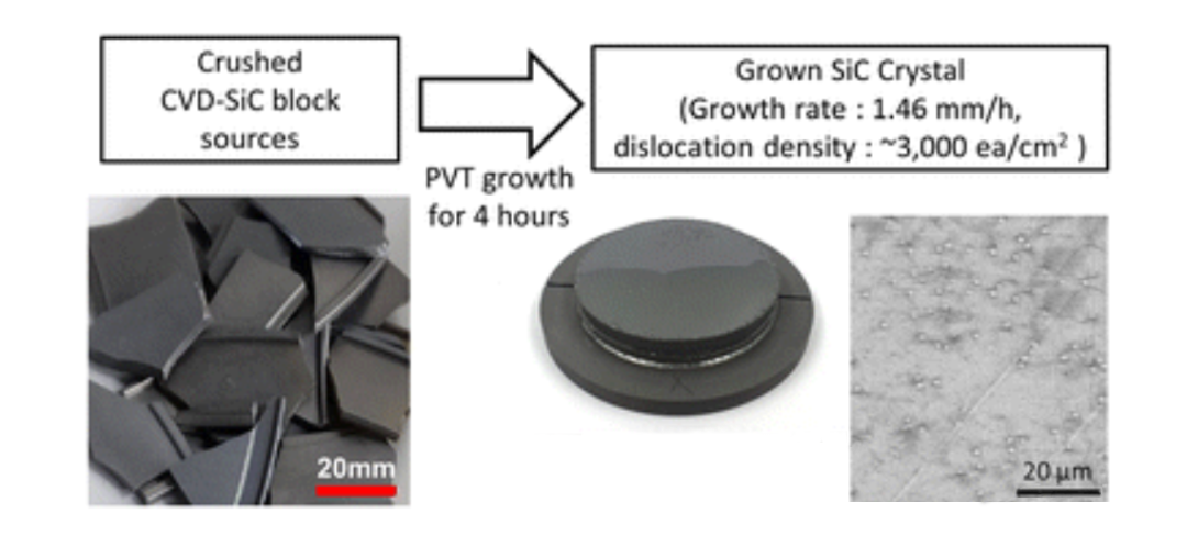
Illustrative Image (Source: Google Search)
The development of SiC crystals dates back several decades, but only in recent years has the technology matured sufficiently for commercial-scale substrate production. Initially, SiC was valued mainly for abrasive and refractory applications, but its potential as a wide bandgap semiconductor has transformed its role in electronics.
The Physical Vapor Transport (PVT) method, established in the late 20th century, became the cornerstone of SiC crystal manufacturing, enabling the production of large-diameter wafers suitable for power device fabrication. Over the past two decades, intensive research and industrial efforts—particularly in Asia and Europe—have reduced defect densities and improved wafer uniformity.
Despite technological advances, SiC substrates remain costly and challenging to produce, with slow growth rates and stringent crystallographic controls limiting yield and scale. However, the increasing global emphasis on energy-efficient electronics and electric mobility is driving rapid innovation and capacity expansion.
For international B2B buyers, understanding this evolutionary context highlights the importance of partnering with experienced suppliers capable of delivering consistent quality while navigating the sector’s inherent technical complexities and market fluctuations.
How can I effectively vet suppliers of SiC crystals to ensure quality and reliability?
Vetting SiC crystal suppliers requires a multi-step approach. Start by verifying their certifications such as ISO 9001 for quality management and any industry-specific accreditations. Request detailed technical datasheets and samples to evaluate crystal quality, including defect densities and polytype consistency. Assess their production capacity and track record with international clients, especially those in your region. Visiting manufacturing facilities or requesting virtual tours can provide transparency. Additionally, check references and review past delivery performance to mitigate risks associated with quality and timeliness.
Is customization of SiC crystal substrates available, and what specifications can typically be tailored?
Yes, many suppliers offer customization to meet specific device requirements. Common customizable parameters include crystal polytype (e.g., 4H-SiC, 6H-SiC), doping type (n-type, p-type, semi-insulating), wafer diameter (4-6 inches typically), thickness, resistivity levels, and surface orientation. Custom doping concentrations and special surface treatments for epitaxial growth can also be negotiated. Early engagement with the supplier to discuss your application needs ensures the tailored product aligns with your device performance and reliability goals.
What are typical minimum order quantities (MOQs), lead times, and payment terms for international SiC crystal orders?
MOQs vary but often start from small batch orders (5-10 wafers) for initial qualification, scaling up for volume production. Lead times depend on crystal size, customization, and supplier capacity, generally ranging from 6 to 12 weeks, considering the slow growth rates inherent to SiC crystal manufacturing. Payment terms commonly include a 30%-50% upfront deposit with the balance on delivery or after inspection. Negotiate payment terms carefully to balance cash flow and supplier trust, especially when dealing across continents.
Illustrative Image (Source: Google Search)
What quality assurance processes and certifications should international buyers expect from reputable SiC crystal suppliers?
Reputable suppliers implement stringent quality assurance including in-process inspections, defect density measurements, and electrical property testing. Certifications to look for include ISO 9001 (quality management), ISO 14001 (environmental management), and RoHS compliance. Suppliers may also provide third-party lab reports validating defect densities, polytype purity, and doping levels. Consistent batch traceability and warranty clauses are critical to address potential defects or deviations in performance.
What logistics considerations are critical when importing SiC crystals from suppliers in Asia or Europe to regions like Africa or South America?
SiC crystals are fragile and require specialized packaging to prevent contamination and mechanical damage during transit. Choose suppliers experienced in international shipping with secure, anti-static, and moisture-controlled packaging. Air freight is preferred for speed but can be costly; sea freight requires additional care for humidity control. Clear customs documentation, import licenses, and compliance with local regulations are essential to avoid delays. Partner with freight forwarders familiar with high-value semiconductor materials to streamline delivery.
How can B2B buyers manage risks related to product defects or delivery disputes in international SiC crystal transactions?
Mitigate risks by establishing clear contracts detailing product specifications, inspection criteria, and dispute resolution mechanisms. Insist on inspection rights either onsite or via third-party labs before shipment. Incorporate penalty clauses for delayed deliveries or quality non-conformance. Maintain open communication channels and document all correspondences. Utilizing escrow payment services or Letters of Credit can safeguard payments. In case of disputes, arbitration under internationally recognized bodies such as ICC can provide neutral resolution.
What are the main cost drivers for SiC crystals, and how can buyers negotiate better pricing without compromising quality?
High growth temperatures, slow crystal growth rates, and defect control contribute to SiC’s high cost structure. Additionally, wafer diameter and customization complexity influence pricing. Buyers can negotiate better terms by committing to larger volumes or longer-term contracts, which incentivize suppliers to optimize production. Consolidating orders with fewer suppliers may yield discounts. Prioritizing standardized specifications over niche customizations can reduce costs. Transparency about your application and volume forecast helps suppliers propose cost-effective solutions.
Are there regional differences in SiC crystal availability or quality that buyers from Africa, South America, the Middle East, and Europe should consider?
Yes, regional factors affect supply chains and quality consistency. Asian suppliers, particularly in China and Japan, lead in volume and innovation but may have longer lead times to Africa and South America due to logistics. European suppliers often provide premium quality with robust certifications but at higher prices. Middle Eastern buyers should consider trade agreements and import duties affecting cost and delivery. Understanding local market dynamics, including available technical support and after-sales services, is crucial to making informed sourcing decisions.
The information provided in this guide, including content regarding manufacturers, technical specifications, and market analysis, is for informational and educational purposes only. It does not constitute professional procurement advice, financial advice, or legal advice.
While we have made every effort to ensure the accuracy and timeliness of the information, we are not responsible for any errors, omissions, or outdated information. Market conditions, company details, and technical standards are subject to change.
B2B buyers must conduct their own independent and thorough due diligence before making any purchasing decisions. This includes contacting suppliers directly, verifying certifications, requesting samples, and seeking professional consultation. The risk of relying on any information in this guide is borne solely by the reader.
Silicon carbide (SiC) crystals represent a critical material foundation for next-generation power electronics, with their superior thermal conductivity and electronic properties driving innovation across high-frequency and high-power device markets. For international B2B buyers, particularly in Africa, South America, the Middle East, and Europe, strategic sourcing of SiC substrates hinges on prioritizing quality, defect minimization, and supplier technological capability. Key factors include understanding the nuances of crystal growth methods—especially the dominant Physical Vapor Transport (PVT) technique—and evaluating suppliers’ success in reducing dislocation densities and controlling polytype purity to enhance device performance and reliability.
Given the high value concentration in SiC substrates and epitaxial layers, buyers must engage closely with manufacturers offering transparent quality metrics and scalable production capacities. This enables informed decisions that balance cost with long-term supply security and product excellence. Additionally, leveraging partnerships with innovative suppliers who invest in advanced crystal growth technologies can unlock competitive advantages in emerging and established markets alike.
Looking ahead, as SiC technology continues to evolve, buyers are encouraged to adopt a forward-thinking sourcing strategy—integrating comprehensive supplier audits, fostering collaborative R&D efforts, and aligning procurement with regional growth trends. This proactive approach will ensure resilience against supply chain disruptions while capitalizing on expanding opportunities in electric vehicles, renewable energy, and high-power industrial applications worldwide.
Tags: Black Silicon Carbide, White Fused Alumina, Brown Fused Alumina, Pink Fused Alumina, Black Fused Alumina